|
数据搜索系统,热门电子元器件搜索 |
|
|
数据搜索系统,热门电子元器件搜索 |
|
SSM2319CBZ-R2 数据表(PDF) 16 Page - Analog Devices |
|
|
|||||||||||||||||||||||||||||
SSM2319CBZ-R2 数据表(HTML) 16 Page - Analog Devices |
|
|
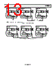
16 / 20 page  SSM2319 Rev. 0 | Page 16 of 20 Operating Modes • SYNCI = external clock. SYNCO is a buffered clock output sourced from an external clock signal. One clock cycle after the internal modulator detect signal is released, an irregular pulse appears on MCLK before the first buffered output signal begins on SYNCO, as shown in Figure 39. The SYNC operating modes include the following: • Initial SYNC startup. An internal reference signal, REF, is released after one complete internal clock cycle (MCLK). After REF is released, another internal signal, MOD, waits 127 internal clock cycles. This operates as a training signal to determine the SYNCI/SYNCO connection. During this time, SYNCO is the internal clock signal. SD REF MOD SYNCI SYNCO MCLK INTERNAL SIGNAL SYNCI = CLKIN • SYNCI = GND or VDD. SYNCO stops generating pulses. The modulator is controlled by an internal clock signal, as shown in Figure 37. SD REF MOD SYNCI SYNCO MCLK INTERNAL SIGNAL SYNCI = GND Figure 39. SYNCI = External Clock • SYNCI = GND, transitions to clock. When the SYNCI pin is connected to GND first but then transitions to a clock signal, SYNCO generates several internal clock signals before finally being synchronized to the external clock signal, as shown in Figure 40. SD REF MOD SYNCI SYNCO MCLK INTERNAL SIGNAL SYNCI = GND TO CLKIN Figure 37. SYNCI = GND or VDD • SYNCI = SYNCO. SYNCO is the delayed clock signal of SYNCI, as shown in Figure 38. SD REF MOD SYNCI SYNCO MCLK INTERNAL SIGNAL SYNCI = SYNCO Figure 40. SYNCI = GND to Clock Input • SYNCI = CLK, transitions to GND. When SYNCI is connected to a clock signal but then transitions to GND, the SYNCO pin immediately stops generating a clock signal. After a short clock loss detect time, the internal modulator synchronizes to the internal clock signal, as shown in Figure 41. Figure 38. SYNCI = SYNCO SD REF MOD SYNCI SYNCO MCLK INTERNAL SIGNAL SYNCI = CLKIN TO GND CLK LOSS DETECT Figure 41. SYNCI = Clock Input to GND |
|
|
链接网址 |
| ALLDATASHEET是否为您带来帮助? [ DONATE ] |
关于 Alldatasheet | 广告服务 | 联系我们 | 隐私政策 | 数据表链接 | 链接交换 | 制造商名单 All Rights Reserved©Alldatasheet.com |
| Russian : Alldatasheetru.com | Korean : Alldatasheet.co.kr | Spanish : Alldatasheet.es | French : Alldatasheet.fr | Italian : Alldatasheetit.com Portuguese : Alldatasheetpt.com | Polish : Alldatasheet.pl | Vietnamese : Alldatasheet.vn Indian : Alldatasheet.in | Mexican : Alldatasheet.com.mx | British : Alldatasheet.co.uk | New Zealand : Alldatasheet.co.nz |
|
Family Site : ic2ic.com |
icmetro.com |
 Chinese ▼
 English
 Chinese
 German
 Japanese
 Russian
 Korean
 Spanish
 French
 Italian
 Portuguese
 Polish
 Vietnamese
 Indian
 Mexican
 British
 New Zealand