|
数据搜索系统,热门电子元器件搜索 |
|
|
数据搜索系统,热门电子元器件搜索 |
|
ADCLK944BCPZ-R2 数据表(PDF) 3 Page - Analog Devices |
|
|
|||||||||||||||||||||||||||||
ADCLK944BCPZ-R2 数据表(HTML) 3 Page - Analog Devices |
|
|
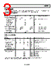
3 / 12 page  ADCLK944 Rev. 0 | Page 3 of 12 SPECIFICATIONS Typical values are given for VCC − VEE = 3.3 V and TA = 25°C, unless otherwise noted. Minimum and maximum values are given for the full VCC − VEE = 3.3 V + 10% to 2.5 V − 5% and TA = −40°C to +85°C variation, unless otherwise noted. CLOCK INPUTS AND OUTPUTS Table 1. Parameter Symbol Min Typ Max Unit Test Conditions/Comments DC INPUT CHARACTERISTICS Input Common-Mode Voltage VICM VEE + 1.35 VCC − 0.1 V Input Differential Voltage VID 0.4 3.4 V p-p ±1.7 V between input pins Input Capacitance CIN 0.4 pF Input Resistance RIN Single-Ended Mode 50 Ω Differential Mode 100 Ω Common Mode 50 kΩ VT open Input Bias Current 20 μA DC OUTPUT CHARACTERISTICS Output Voltage High Level VOH VCC − 1.26 VCC − 0.76 V Load = 50 Ω to (VCC − 2.0 V) Output Voltage Low Level VOL VCC − 1.99 VCC − 1.54 V Load = 50 Ω to (VCC − 2.0 V) Output Voltage, Single-Ended VO 600 960 mV VOH − VOL, output static Voltage Reference VREF Output Voltage (VCC + 1)/2 V −500 μA to +500 μA Output Resistance 250 Ω TIMING CHARACTERISTICS Table 2. Parameter Symbol Min Typ Max Unit Test Conditions/Comments AC PERFORMANCE Maximum Output Frequency 6.2 7.0 GHz Differential output voltage swing > 0.8 V (see Figure 4) Output Rise/Fall Time tR 35 50 75 ps 20% to 80%, measured differentially Propagation Delay tPD 70 100 130 ps VID = 1.6 V p-p Temperature Coefficient 75 fs/°C Output-to-Output Skew1 15 ps Part-to-Part Skew 35 ps VID = 1.6 V p-p Additive Time Jitter Integrated Random Jitter 26 fs rms BW = 12 kHz to 20 MHz, CLK = 1 GHz Broadband Random Jitter2 50 fs rms VID = 1.6 V p-p, 8 V/ns, VICM = 2 V CLOCK OUTPUT PHASE NOISE Absolute Phase Noise Input slew rate > 1 V/ns (see Figure 11) fIN = 1 GHz −118 dBc/Hz 100 Hz offset −135 dBc/Hz 1 kHz offset −144 dBc/Hz 10 kHz offset −150 dBc/Hz 100 kHz offset −150 dBc/Hz >1 MHz offset 1 The output-to-output skew is the difference between any two similar delay paths while operating at the same voltage and temperature. 2 Measured at the rising edge of the clock signal; calculated using the SNR of the ADC method. |
|
|
链接网址 |
| ALLDATASHEET是否为您带来帮助? [ DONATE ] |
关于 Alldatasheet | 广告服务 | 联系我们 | 隐私政策 | 数据表链接 | 链接交换 | 制造商名单 All Rights Reserved©Alldatasheet.com |
| Russian : Alldatasheetru.com | Korean : Alldatasheet.co.kr | Spanish : Alldatasheet.es | French : Alldatasheet.fr | Italian : Alldatasheetit.com Portuguese : Alldatasheetpt.com | Polish : Alldatasheet.pl | Vietnamese : Alldatasheet.vn Indian : Alldatasheet.in | Mexican : Alldatasheet.com.mx | British : Alldatasheet.co.uk | New Zealand : Alldatasheet.co.nz |
|
Family Site : ic2ic.com |
icmetro.com |
 Chinese ▼
 English
 Chinese
 German
 Japanese
 Russian
 Korean
 Spanish
 French
 Italian
 Portuguese
 Polish
 Vietnamese
 Indian
 Mexican
 British
 New Zealand