|
数据搜索系统,热门电子元器件搜索 |
|
|
数据搜索系统,热门电子元器件搜索 |
|
ADL5902ACPZ-R2 数据表(PDF) 15 Page - Analog Devices |
|
|
|||||||||||||||||||||||||||||
ADL5902ACPZ-R2 数据表(HTML) 15 Page - Analog Devices |
|
|
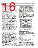
15 / 28 page  ADL5902 Rev. 0 | Page 15 of 28 THEORY OF OPERATION The ADL5902 is a 50 MHz to 9 GHz true rms responding detector with a 65 dB measurement range at 2.14 GHz and a greater than 56 dB measurement range at frequencies up to 6 GHz. It incorporates a modified AD8362 architecture that increases the frequency range and improves measurement accuracy at high frequencies. Transfer function peak-to-peak ripple has been reduced to <±0.1 dB over the entire dynamic range. Temperature stability of the rms output measurements provides <±0.3 dB error, typically, over the specified temperature range of −40°C to 125°C through proprietary techniques. The device accurately measures waveforms that have a high peak-to- rms ratio (crest factor). The ADL5902 consists of a high performance AGC loop. As shown in Figure 36, the AGC loop comprises a wide bandwidth variable gain amplifier (VGA), square law detectors, an amplitude target circuit, and an output driver. For a more detailed description of the functional blocks, see the AD8362 data sheet. The nomenclature used in this data sheet to distinguish between a pin name and the signal on that pin is as follows: • The pin name is all uppercase, for example, VPOS, COMM, and VOUT. • The signal name or a value associated with that pin is the pin mnemonic with a partial subscript, for example, CLPF and VOUT. SQUARE LAW DETECTOR AND AMPLITUDE TARGET The VGA gain has the form GSET = GO e ) / ( GNS SET V V − (1) where: GO is the basic fixed gain. VGNS is a scaling voltage that defines the gain slope (the decibel change per voltage). The gain decreases with increasing VSET. The VGA output is VSIG = GSET × RFIN = GO × RFIN e ) / ( GNS SET V V − (2) where RFIN is the ac voltage applied to the input terminals of the ADL5902. The output of the VGA, VSIG, is applied to a wideband square law detector. The detector provides the true rms response of the RF input signal, independent of waveform. The detector output, ISQR, is a fluctuating current with positive mean value. The difference between ISQR and an internally generated current, ITGT, is integrated by the parallel combination of CF and the external capacitor attached to the CLPF pin at the summing node. CF is an on-chip 26 pF filter capacitor, and CLPF, the external capacitance connected to the CLPF pin, can be used to arbitrarily increase the averaging time while trading off with the response time. When the AGC loop is at equilibrium Mean(ISQR) = ITGT (3) This equilibrium occurs only when Mean(VSIG2) = VTGT2 (4) where VTGT is the voltage presented at the VTGT pin. This pin can conveniently be connected to the VREF pin through a voltage divider to establish a target rms voltage, VATG, of ~40 mV rms when VTGT = 0.8 V. Because the square law detectors are electrically identical and well matched, process and temperature dependent variations are effectively cancelled. TADJ/PWDN BAND GAP REFERENCE COMM VOUT TEMP (1.4V) VREF (2.3V) ISQR ITGT X2 X2 GSET CLPF (EXTERNAL) CF (INTERNAL) VSIG VGA SUMMING NODE VSET CH (INTERNAL) VPOS INHI INLO TEMPERATURE COMPENSATION AND BIAS TEMPERATURE SENSOR VTGT CLPF VATG = VTGT 20 Figure 36. Simplified Architecture Details |
|
|
链接网址 |
| ALLDATASHEET是否为您带来帮助? [ DONATE ] |
关于 Alldatasheet | 广告服务 | 联系我们 | 隐私政策 | 数据表链接 | 链接交换 | 制造商名单 All Rights Reserved©Alldatasheet.com |
| Russian : Alldatasheetru.com | Korean : Alldatasheet.co.kr | Spanish : Alldatasheet.es | French : Alldatasheet.fr | Italian : Alldatasheetit.com Portuguese : Alldatasheetpt.com | Polish : Alldatasheet.pl | Vietnamese : Alldatasheet.vn Indian : Alldatasheet.in | Mexican : Alldatasheet.com.mx | British : Alldatasheet.co.uk | New Zealand : Alldatasheet.co.nz |
|
Family Site : ic2ic.com |
icmetro.com |
 Chinese ▼
 English
 Chinese
 German
 Japanese
 Russian
 Korean
 Spanish
 French
 Italian
 Portuguese
 Polish
 Vietnamese
 Indian
 Mexican
 British
 New Zealand