|
数据搜索系统,热门电子元器件搜索 |
|
|
数据搜索系统,热门电子元器件搜索 |
|
ADL5902ACPZ-R2 数据表(PDF) 16 Page - Analog Devices |
|
|
|||||||||||||||||||||||||||||
ADL5902ACPZ-R2 数据表(HTML) 16 Page - Analog Devices |
|
|
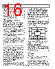
16 / 28 page  ADL5902 Rev. 0 | Page 16 of 28 When forcing the previous identity by varying the VGA setpoint, it is apparent that RMS(VSIG) = √(Mean(VSIG2)) = √(VATG2) = VATG (5) Substituting the value of VSIG from Equation 2 results in RMS(G0 × RFIN e ) / ( GNS SET V V ) = VATG (6) When connected as a measurement device, VSET = VOUT. Solving for VOUT as a function of RFIN, VOUT = VSLOPE × log10(RMS(RFIN)/VZ) (7) where: VSLOPE is 1.06 V/decade (or 53 mV/dB) at 2.14 GHz. VZ is the intercept voltage. When RMS(RFIN) = VZ, this implies that VOUT = 0 V because log10(1) = 0. This makes the intercept the input that forces VOUT = 0 V if the ADL5902 had no sensitivity limit. The PINTERCEPT (in decibels relative to 1 milliwatt, that is, dBm) corresponding to Vz (in volts) in ADL5902 is given by the following equation: PINTERCEPT = −(VPEDISTAL/VSLOPE) + PMINDET (8) where VPEDISTAL is the VSET interface’s pedestal voltage, and PMINDET is the minimum detectable signal in decibels relative to 1 milliwatt, given by the following expression: PMINDET = dBm (VATG) – GO (9) where dBm(VATG) is the equivalent power in decibels relative to 1 milliwatt corresponding to a given VTGT. Combining Equation 8 and Equation 9 results in PINTERCEPT = −(VPEDISTAL/VSLOPE) + dBm (VATG) – GO (10) For the ADL5902, VPEDISTAL is approximately 0.275 V and VATG is given by VTGT/20. GO is 45 dB below approximately 4 GHz and then decreases at higher frequencies. VTGT = 0.8 V; therefore, VATG = 40 mV and dBm (VATG) = 10 log10((40 mV)2/50 Ω)/1 mW) ≈ −14.9 dBm At 2.14 GHz, VSLOPE ≈ 53 mV/dB and GO at 2.14 GHz = 45 dB. This results in a PINTERCEPT ≈ −65 dBm. This differs slightly from the value in Table 1 due to the choice of calibration points and the slight nonideality of the response. In most applications, the AGC loop is closed through the setpoint interface and the VSET pin. In measurement mode, VOUT is directly connected to VSET (see the Measurement Mode Basic Connections section for more information). In controller mode, a control voltage is applied to VSET, and the VOUT pin typically drives the control input of an amplification or attenuation system. In this case, the voltage at the VSET pin forces a signal amplitude at the RF inputs of the ADL5902 that balances the system through feedback. RF INPUT INTERFACE Figure 37 shows the RF input connections within the ADL5902. The input impedance is set primarily by an internal 2 kΩ resistor connected between INHI and INLO. A dc level of approximately half the supply voltage on each pin is established internally. Either the INHI or INLO pin can be used as the single-ended RF input pin. Signal coupling capacitors must be connected from the input signal to the INHI and INLO pins. A single external 60.4 Ω resistor to ground from the desired input creates an equivalent 50 Ω impedance over a broad section of the operating frequency range. The other input pin should be RF ac-coupled to common (ground). The input signal high-pass corner formed by the input coupling capacitor’s internal and external resistances is fHIGHPASS = 1/(2 × π × 50 × C) (11) where C is the capacitance in farads and fHIGHPASS is in hertz. The input coupling capacitors must be large enough in value to pass the input signal frequency of interest and determine the low end of the frequency response. INHI and INLO can also be driven differentially using a balun. ESD ESD ESD ESD ESD ESD ESD ESD ESD ESD ESD ESD ESD INLO INHI VPOS COMM VBIAS LOAD 2k Ω 2k Ω Figure 37. RF Inputs Extensive ESD protection is employed on the RF inputs, and this protection limits the maximum possible input to the ADL5902. SMALL SIGNAL LOOP RESPONSE The ADL5902 uses a VGA in a loop to force a squared RF signal to be equal to a squared dc voltage. This nonlinear loop can be simplified and solved for a small signal loop response. The low- pass corner pole is given by FreqLP ≈ 1.83 × ITGT/(CLPF) (12) where: ITGT is in amperes. CLPF is in farads. FreqLP is in hertz. ITGT is derived from VTGT; however, ITGT is a squared value of VTGT multiplied by a transresistance, namely ITGT = gm × VTGT2 (13) gm is approximately 18.9 μs; therefore, with VTGT equal to the typically recommended 0.8 V, ITGT is approximately 12 μA. The value of this current varies with temperature; therefore, the small signal pole varies with temperature. However, because the RF squaring circuit and dc squaring circuit track with temperature, |
|
|
链接网址 |
| ALLDATASHEET是否为您带来帮助? [ DONATE ] |
关于 Alldatasheet | 广告服务 | 联系我们 | 隐私政策 | 数据表链接 | 链接交换 | 制造商名单 All Rights Reserved©Alldatasheet.com |
| Russian : Alldatasheetru.com | Korean : Alldatasheet.co.kr | Spanish : Alldatasheet.es | French : Alldatasheet.fr | Italian : Alldatasheetit.com Portuguese : Alldatasheetpt.com | Polish : Alldatasheet.pl | Vietnamese : Alldatasheet.vn Indian : Alldatasheet.in | Mexican : Alldatasheet.com.mx | British : Alldatasheet.co.uk | New Zealand : Alldatasheet.co.nz |
|
Family Site : ic2ic.com |
icmetro.com |
 Chinese ▼
 English
 Chinese
 German
 Japanese
 Russian
 Korean
 Spanish
 French
 Italian
 Portuguese
 Polish
 Vietnamese
 Indian
 Mexican
 British
 New Zealand