|
数据搜索系统,热门电子元器件搜索 |
|
|
数据搜索系统,热门电子元器件搜索 |
|
LPC2157 数据表(PDF) 9 Page - NXP Semiconductors |
|
|
|||||||||||||||||||||||||||||
LPC2157 数据表(HTML) 9 Page - NXP Semiconductors |
|
|
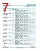
9 / 45 page  LPC2157_2158_2 © NXP B.V. 2009. All rights reserved. Product data sheet Rev. 02 — 9 February 2009 9 of 45 NXP Semiconductors LPC2157/2158 Single-chip 16-bit/32-bit microcontrollers [1] 5 V tolerant pad providing digital I/O functions with TTL levels and hysteresis and 10 ns slew rate control. [2] 5 V tolerant pad providing digital I/O functions with TTL levels and hysteresis and 10 ns slew rate control. If configured for an input function, this pad utilizes built-in glitch filter that blocks pulses shorter than 3 ns. [3] Open-drain 5 V tolerant digital I/O I2C-bus 400 kHz specification compatible pad. It requires external pull-up to provide an output functionality. [4] 5 V tolerant pad providing digital I/O (with TTL levels and hysteresis and 10 ns slew rate control) and analog input function. If configured for an input function, this pad utilizes built-in glitch filter that blocks pulses shorter than 3 ns. When configured as an ADC input, digital section of the pad is disabled. [5] 5 V tolerant pad providing digital I/O (with TTL levels and hysteresis and 10 ns slew rate control) and analog output function. When configured as the DAC output, digital section of the pad is disabled. [6] 5 V tolerant pad with built-in pull-up resistor providing digital I/O functions with TTL levels and hysteresis and 10 ns slew rate control. The pull-up resistor’s value typically ranges from 60 k Ω to 300 kΩ. [7] Pad is designed in accordance with the Universal Serial Bus (USB) specification, revision 2.0 (Full-speed and Low-speed mode only). [8] 5 V tolerant pad providing digital input (with TTL levels and hysteresis) function only. [9] Pad provides special analog functionality. RESET 83[8] I External reset input: A LOW on this pin resets the device, causing I/O ports and peripherals to take on their default states, and processor execution to begin at address 0. TTL with hysteresis, 5 V tolerant. XTAL1 88[9] O Input from the oscillator amplifier. XTAL2 87[9] I Output to the oscillator circuit and internal clock generator circuits. RTCX1 93[9] I Input to the RTC oscillator circuit. RTCX2 94[9] O Output from the RTC oscillator circuit. VSS 6, 13, 32, 39, 40, 85, 95 I Ground: 0 V reference. VDD 11, 27, 33 I 3.3 V power supply: This is the power supply voltage for the core and I/O ports. VDDA 96 I Analog 3.3 V power supply: This should be nominally the same voltage as VDD but should be isolated to minimize noise and error. This voltage is only used to power the on-chip ADC(s) and DAC. VDD(LCD) 38 I 1.8 V to 5.5 V power supply: Power supply voltage for the PCF8576D. VLCD 41 I LCD power supply: LCD voltage. VREF 89 I ADC reference voltage: This should be nominally less than or equal to the VDD voltage but should be isolated to minimize noise and error. Level on this pin is used as a reference for ADC(s) and DAC. VBAT 31 I RTC power supply voltage: 3.3 V on this pin supplies the power to the RTC. SDA_LCD 34 I/O SDA LCD — I2C-bus data signal for the LCD controller. SCL_LCD 35 I SCL LCD — I2C-bus clock signal for the LCD controller. SYNC 36 I/O SYNC — cascade synchronization input/output CLK 37 I/O CLK — external clock input/output BP0 to BP3 42 to 45 O BP0 to BP3: LCD backplane outputs. S0 to S31 46 to 77 O S0 to S31: LCD segment outputs. Table 2. Pin description LPC2157 …continued Symbol Pin Type Description |
|
链接网址 |
| ALLDATASHEET是否为您带来帮助? [ DONATE ] |
关于 Alldatasheet | 广告服务 | 联系我们 | 隐私政策 | 数据表链接 | 链接交换 | 制造商名单 All Rights Reserved©Alldatasheet.com |
| Russian : Alldatasheetru.com | Korean : Alldatasheet.co.kr | Spanish : Alldatasheet.es | French : Alldatasheet.fr | Italian : Alldatasheetit.com Portuguese : Alldatasheetpt.com | Polish : Alldatasheet.pl | Vietnamese : Alldatasheet.vn Indian : Alldatasheet.in | Mexican : Alldatasheet.com.mx | British : Alldatasheet.co.uk | New Zealand : Alldatasheet.co.nz |
|
Family Site : ic2ic.com |
icmetro.com |
 Chinese ▼
 English
 Chinese
 German
 Japanese
 Russian
 Korean
 Spanish
 French
 Italian
 Portuguese
 Polish
 Vietnamese
 Indian
 Mexican
 British
 New Zealand