|
数据搜索系统,热门电子元器件搜索 |
|
|
数据搜索系统,热门电子元器件搜索 |
|
AD8352ACPZ-R2 数据表(PDF) 12 Page - Analog Devices |
|
|
|||||||||||||||||||||||||||||
AD8352ACPZ-R2 数据表(HTML) 12 Page - Analog Devices |
|
|
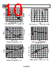
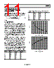
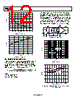
12 / 20 page  AD8352 Rev. B | Page 12 of 20 20 0 0 800 RG (Ω) 18 16 14 12 10 8 6 4 2 100 200 300 400 500 600 700 Figure 24. Gain vs. RG, RL = 1 kΩ 20 0 00 CD (pF) .5 18 16 14 12 10 8 6 4 2 0.1 0.2 0.3 0.4 Figure 25. Gain vs. CD, RL = 1 kΩ SINGLE-ENDED INPUT OPERATION The AD8352 can be configured as a single-ended-to-differential amplifier, as shown in Figure 26. To balance the outputs when driving the VIP input, an external resistor (RN) of 200 Ω is added between VIP and RGN. See Equation 2 to determine the single- ended input gain (AV Single-Ended) for a given RG or RL. 30 430 ) 53 ( ) 5 ( 500 + + ⎟⎟ ⎠ ⎞ ⎜⎜ ⎝ ⎛ + + + + = − L L L L G G Ended Single V R R R R R R A (2) where RL is the single-ended load. RG is the gain setting resistor. Figure 27 plots gain vs. RG for 200 Ω and 1 kΩ loads. Table 7 and Table 8 show the values of CD and RD required (for 180 MHz broadband, third-order, single tone optimization) for 200 Ω and 1 kΩ loads, respectively. This single-ended configuration provides −3 dB bandwidths similar to input differential drive. Figure 28 through Figure 31 show distortion levels at a gain of 12 dB for both 200 Ω and 1 kΩ loads. Gains from 3 dB to 18 dB, using optimized CD and RD values, obtain similar distortion levels. RD RG 25Ω 65Ω 50Ω 0.1µF 0.1µF 0.1µF 0.1µF RGP RGN AD8352 AC CD VIP RN 200Ω Figure 26. Single-Ended Schematic 40 0 1 10k RG (Ω) 10 100 1k 35 30 25 20 15 10 5 GAIN, RL =1kΩ GAIN, RL =200Ω Figure 27. Gain vs. RG –60 –110 FREQUENCY (MHz) 10 70 140 190 240 –70 –80 –90 –100 2V p-p OUT 1V p-p OUT Figure 28. Single-Ended, Second-Order Harmonic Distortion (HD2) vs. Frequency, 200 Ω Load |
|
|
链接网址 |
| ALLDATASHEET是否为您带来帮助? [ DONATE ] |
关于 Alldatasheet | 广告服务 | 联系我们 | 隐私政策 | 数据表链接 | 链接交换 | 制造商名单 All Rights Reserved©Alldatasheet.com |
| Russian : Alldatasheetru.com | Korean : Alldatasheet.co.kr | Spanish : Alldatasheet.es | French : Alldatasheet.fr | Italian : Alldatasheetit.com Portuguese : Alldatasheetpt.com | Polish : Alldatasheet.pl | Vietnamese : Alldatasheet.vn Indian : Alldatasheet.in | Mexican : Alldatasheet.com.mx | British : Alldatasheet.co.uk | New Zealand : Alldatasheet.co.nz |
|
Family Site : ic2ic.com |
icmetro.com |
 Chinese ▼
 English
 Chinese
 German
 Japanese
 Russian
 Korean
 Spanish
 French
 Italian
 Portuguese
 Polish
 Vietnamese
 Indian
 Mexican
 British
 New Zealand