|
数据搜索系统,热门电子元器件搜索 |
|
|
数据搜索系统,热门电子元器件搜索 |
|
AD8352ACPZ-R2 数据表(PDF) 15 Page - Analog Devices |
|
|
|||||||||||||||||||||||||||||
AD8352ACPZ-R2 数据表(HTML) 15 Page - Analog Devices |
|
|
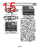
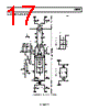
15 / 20 page  AD8352 Rev. B | Page 15 of 20 AD8352 50Ω 0Ω 0Ω CD RD RG 0.1µF 0.1µF 0.1µF 0.1µF 16 1 2 3 4 5 24Ω 0.1µF 10 24Ω 0.1µF 11 8, 13 14 VCC AD9445 IF/RF INPUT ADT1-1WT FREQUENCY (MHz) 0 –150 052.50 –10 –20 –30 –40 –50 –60 –70 –80 –90 –100 –110 –120 –130 –140 5.25 10.50 15.75 21.00 26.25 31.50 36.75 42.00 47.25 SNR = 61.98dBc NOISE FLOOR = –111.2dB FUND1 = –7.072dBFS FUND2 = –7.043dBFS IMD (2F2-F1) = –89dBc IMD (2F1-F2) = –88dBc Figure 34. Differential Input to the AD8352 Driving the AD9445 RD RG 25Ω 50Ω 50Ω AD8352 CD 33Ω 33Ω 0.1µF 0.1µF 0.1µF 0.1µF AC VIP VIN VOP VON RN 200Ω AD9445 VIN+ VIN– Figure 37. Two Tone Distortion AD8352 Driving AD9445, Encode Clock @ 105 MHz with fC @ 100 MHz (AV = 10 dB), Analog In = 98 MHz and 101 MHz, See Figure 34 LAYOUT AND TRANSMISSION LINE EFFECTS High Q inductive drives and loads, as well as stray transmission line capacitance in combination with package parasitics, can potentially form a resonant circuit at high frequencies resulting in excessive gain peaking or possible oscillation. If RF transmission lines connecting the input or output are used, they should be designed such that stray capacitance at the input/output pins is minimized. In many board designs, the signal trace widths should be minimal where the driver/ receiver is more than one-eighth of the wavelength from the AD8352. This nontransmission line configuration requires that underlying and adjacent ground and low impedance planes be dropped from the signal lines. In a similar fashion, stray capacitance should be minimized near the RG, CD, and RD components and associated traces. This also requires not placing low impedance planes near these components. Refer to the evaluation board layout (Figure 39 and Figure 40) for more information. Excessive stray capacitance at these nodes results in unwanted high frequency distortion. The 0.1 μF supply decoupling capacitors need to be close to the amplifier. This includes Signal Capacitor C2 through Signal Capacitor C5. Figure 35. Single-Ended Input to the AD8352 Driving the AD9445 0 –150 0 52.50 FREQUENCY (MHz) –10 –20 –30 –40 –50 –60 –70 –80 –90 –100 –110 –120 –130 –140 5.25 10.50 15.75 21.00 26.25 31.50 36.75 42.00 47.25 SNR = 67.26dBc SFDR = 83.18dBc NOISE FLOOR = –110.5dB FUND = –1.074dBFS SECOND = –83.14dBc THIRD = –85.39dBc Figure 36. Single Tone Distortion AD8352 Driving AD9445, Encode Clock @ 105 MHz with fC @ 100 MHz (AV = 10 dB), See Figure 34 Parasitic suppressing resistors (R5, R6, R7, and R11) can be used at the device input/output pins. Use 25 Ω series resistors (Size 0402) to adequately de-Q the input and output system from most parasitics without a significant decrease in gain. In general, if proper board layout techniques are used, the suppression resistors are not necessarily required. Output Parasitic Suppression Resistor R7 and Output Parasitic Suppression Resistor R11 can be required for driving some switch capacitor ADCs. These suppressors, with Input C of the converter (and possibly added External Shunt C), help provide charge kickback isolation and improve overall distortion at high encode rates. |
|
|
链接网址 |
| ALLDATASHEET是否为您带来帮助? [ DONATE ] |
关于 Alldatasheet | 广告服务 | 联系我们 | 隐私政策 | 数据表链接 | 链接交换 | 制造商名单 All Rights Reserved©Alldatasheet.com |
| Russian : Alldatasheetru.com | Korean : Alldatasheet.co.kr | Spanish : Alldatasheet.es | French : Alldatasheet.fr | Italian : Alldatasheetit.com Portuguese : Alldatasheetpt.com | Polish : Alldatasheet.pl | Vietnamese : Alldatasheet.vn Indian : Alldatasheet.in | Mexican : Alldatasheet.com.mx | British : Alldatasheet.co.uk | New Zealand : Alldatasheet.co.nz |
|
Family Site : ic2ic.com |
icmetro.com |
 Chinese ▼
 English
 Chinese
 German
 Japanese
 Russian
 Korean
 Spanish
 French
 Italian
 Portuguese
 Polish
 Vietnamese
 Indian
 Mexican
 British
 New Zealand