|
数据搜索系统,热门电子元器件搜索 |
|
|
数据搜索系统,热门电子元器件搜索 |
|
AD8420ARMZ-R7 数据表(PDF) 9 Page - Analog Devices |
|
|
|||||||||||||||||||||||||||||
AD8420ARMZ-R7 数据表(HTML) 9 Page - Analog Devices |
|
|
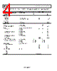
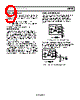
9 / 10 page  Preliminary Technical Data AD8420 Rev. PrD | Page 9 of 9 INPUT VOLTAGE RANGE Unlike traditional instrumentation amplifier architectures, the allowed input range of the AD8420 is simplicity itself. For the AD8420’s transfer function to be valid, the input voltage should follow two rules: 1) Keep differential input voltage within ±1V. 2) Keep voltage on +IN, -IN, and REF pins in specified input voltage range No hexagonal figures. No complicated formulas. INPUT PROTECTION The AD8420 has very robust inputs and typically does not need additional input protection. Input voltages can be up to 40 V from the opposite supply rail. For example, with a +5 V positive supply and a −8 V negative supply, the part can safely withstand voltages from −35 V to 32 V. The part can handle large differential input voltages, even when the part is in high gain, without damage. The rest of the AD8420 terminals should be kept within the supplies. All terminals of the AD8426 are protected against ESD. For applications that require protection beyond the AD8420’s limits, place diodes at the AD8420 inputs to limit voltage and resistors in series with the inputs to limit the current into these diodes. To keep input bias current at minimum, low leakage diode clamps such as the BAV199 should be used. The AD8420 also combines well with TVS diodes such as the PTVSxS1UR. DRIVING THE REFERENCE PIN Traditional instrumentation amplifier architectures require the reference pin to be driven with a low impedance source. In traditional architectures, impedance at the reference pin degrades both CMRR and gain accuracy. With the AD8420 architecture, resistance at the reference pin has no effect on CMRR. –IN +IN VREF RREF R2 R1 G = 1+ R2+RREF R1 AD8420 VOUT REF FB Figure 5. Calculating Gain with Reference Resistance Resistance at the reference pin does affect the AD8420’s gain, but if this resistance is constant, the gain setting resistors can be adjusted to compensate. For example, the AD8420 can be driven with a voltage divider as shown in Figure 6. –IN +IN VS R2 R1 G = 1+ R2+R3||R4 R1 AD8420 VOUT REF FB R4 R3 Optional capacitor filters noise from Vs Figure 6. Using Resistor Divider to Set Reference Voltage |
|
|
链接网址 |
| ALLDATASHEET是否为您带来帮助? [ DONATE ] |
关于 Alldatasheet | 广告服务 | 联系我们 | 隐私政策 | 数据表链接 | 链接交换 | 制造商名单 All Rights Reserved©Alldatasheet.com |
| Russian : Alldatasheetru.com | Korean : Alldatasheet.co.kr | Spanish : Alldatasheet.es | French : Alldatasheet.fr | Italian : Alldatasheetit.com Portuguese : Alldatasheetpt.com | Polish : Alldatasheet.pl | Vietnamese : Alldatasheet.vn Indian : Alldatasheet.in | Mexican : Alldatasheet.com.mx | British : Alldatasheet.co.uk | New Zealand : Alldatasheet.co.nz |
|
Family Site : ic2ic.com |
icmetro.com |
 Chinese ▼
 English
 Chinese
 German
 Japanese
 Russian
 Korean
 Spanish
 French
 Italian
 Portuguese
 Polish
 Vietnamese
 Indian
 Mexican
 British
 New Zealand