|
数据搜索系统,热门电子元器件搜索 |
|
|
数据搜索系统,热门电子元器件搜索 |
|
ADA4084-2ARMZ-R7 数据表(PDF) 20 Page - Analog Devices |
|
|
|||||||||||||||||||||||||||||
ADA4084-2ARMZ-R7 数据表(HTML) 20 Page - Analog Devices |
|
|
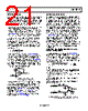
20 / 24 page  ADA4084-2 Data Sheet Rev. A | Page 20 of 24 APPLICATIONS INFORMATION FUNCTIONAL DESCRIPTION The ADA4084-2 is a precision single-supply, rail-to-rail opera- tional amplifier. Intended for portable instrumentation, the ADA4084-2 combines the attributes of precision, wide band- width, and low noise to make it an ideal choice in single-supply applications that require both ac and precision dc performance. Other low supply voltage applications for which the ADA4084-2 is well suited are active filters, audio microphone preamplifiers, power supply control, and telecommunications. To combine all of these attributes with rail-to-rail input/output operation, novel circuit design techniques are used. D2 D101 D100 D5 D4 D1 Q1 Q4 Q3 Q2 R4 R1 R2 R3 Figure 73. ADA4084-2 Equivalent Input Circuit For example, Figure 73 illustrates a simplified equivalent circuit for the input stage of the ADA4084-2. It comprises a PNP differential pair, Q1 and Q2, and an NPN differential pair, Q3 and Q4, operating concurrently. Diode D100 and Diode D101 serve to clamp the applied differential input voltage to the ADA4084-2, thereby protecting the input transistors against Zener breakdown of the emitter-base junctions. Input stage voltage gains are kept low for input rail-to-rail operation. The two pairs of differential output voltages are connected to the second stage of the ADA4084-2, which is a modified compound folded cascade gain stage. It is also in the second gain stage, where the two pairs of differential output voltages are combined into a single-ended output signal voltage used to drive the output stage. A key issue in the input stage is the behavior of the input bias currents over the input common-mode voltage range. Input bias currents in the ADA4084-2 are the arithmetic sum of the base currents in Q1 and Q4 and in Q2 and Q3. As a result of this design approach, the input bias currents in the ADA4084-2 not only exhibit different amplitudes; they also exhibit different polarities. This effect is best illustrated by Figure 7, Figure 8, Figure 30, Figure 31, Figure 53, and Figure 54. It is therefore important that the effective source impedances connected to the ADA4084-2 inputs be balanced for optimum dc and ac performance. To achieve rail-to-rail output, the ADA4084-2 output stage design employs a unique topology for both sourcing and sinking current. This circuit topology is illustrated in Figure 74. The output stage is voltage-driven from the second gain stage. The signal path through the output stage is inverting; that is, for positive input signals, Q13 provides the base current drive to Q19 so that it conducts (sinks) current. For negative input signals, the signal path via Q18 → mirror → Q24 provides the base current drive for Q23 to conduct (source) current. Both transistors provide output current until they are forced into saturation. Q24 Q21 D20 Q13 Q18 Q19 Q23 VEE VOUT VCC VBIAS MIRROR R5 R6 R7 C2 C1 Figure 74. ADA4084-2 Equivalent Output Circuit Thus, the saturation voltage of the output transistors sets the limit on the ADA4084-2 maximum output voltage swing. Output short-circuit current limiting is determined by the maximum signal current into the base of Q13 from the second gain stage. The output stage also exhibits voltage gain. This is accomplished by the use of common-emitter amplifiers, and, as a result, the voltage gain of the output stage (thus, the open-loop gain of the device) exhibits a dependence on the total load resistance at the output of the ADA4084-2. |
|
|
链接网址 |
| ALLDATASHEET是否为您带来帮助? [ DONATE ] |
关于 Alldatasheet | 广告服务 | 联系我们 | 隐私政策 | 数据表链接 | 链接交换 | 制造商名单 All Rights Reserved©Alldatasheet.com |
| Russian : Alldatasheetru.com | Korean : Alldatasheet.co.kr | Spanish : Alldatasheet.es | French : Alldatasheet.fr | Italian : Alldatasheetit.com Portuguese : Alldatasheetpt.com | Polish : Alldatasheet.pl | Vietnamese : Alldatasheet.vn Indian : Alldatasheet.in | Mexican : Alldatasheet.com.mx | British : Alldatasheet.co.uk | New Zealand : Alldatasheet.co.nz |
|
Family Site : ic2ic.com |
icmetro.com |
 Chinese ▼
 English
 Chinese
 German
 Japanese
 Russian
 Korean
 Spanish
 French
 Italian
 Portuguese
 Polish
 Vietnamese
 Indian
 Mexican
 British
 New Zealand