|
数据搜索系统,热门电子元器件搜索 |
|
|
数据搜索系统,热门电子元器件搜索 |
|
ADA4084-2ARMZ-R7 数据表(PDF) 21 Page - Analog Devices |
|
|
|||||||||||||||||||||||||||||
ADA4084-2ARMZ-R7 数据表(HTML) 21 Page - Analog Devices |
|
|
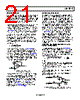
21 / 24 page  Data Sheet ADA4084-2 Rev. A | Page 21 of 24 INPUT PROTECTION As with any semiconductor device, if conditions exist where the applied input voltages to the device exceed either supply voltage, the input overvoltage I-to-V characteristic of the device must be considered. When an overvoltage occurs, the amplifier may be damaged, depending on the magnitude of the applied voltage and the magnitude of the fault current. The D1, D2, D4, and D5 diodes conduct when the input common- mode voltage exceeds either supply pin by a diode drop. This varies with temperature and is in the range of 0.3 V to 0.8 V. As illustrated in the simplified equivalent circuit shown in Figure 73, the ADA4084-2 does not have any internal current limiting resis- tors; thus, fault currents can quickly rise to damaging levels. This input current is not inherently damaging to the device, provided that it is limited to 5 mA or less. If a fault condition causes more than 5 mA to flow, an external series resistor should be added at the expense of additional thermal noise. Figure 75 illustrates a typical noninverting configuration for an overvoltage-protected amplifier where the series resistance, RS, is chosen, such that ( ) mA 5 SUPPLY MAX IN S V V R − = For example, a 1 kΩ resistor protects the ADA4084-2 against input signals up to 5 V above and below the supplies. Note that the thermal noise of a 1 kΩ resistor at room temperature is 4 nV/√Hz, which exceeds the voltage noise of the ADA4084-2. For other configurations where both inputs are used, each input should be protected against abuse with a series resistor. Again, to ensure optimum dc and ac performance, it is recommended that source impedance levels be balanced. R1 R2 VIN VOUT 1/2 ADA4084-2 Figure 75. Resistance in Series with Input Limits Overvoltage Currents to Safe Values To protect Q1-Q2 and Q3-Q4 from large differential voltages that may result in Zener breakdown of the emitter-base junction, D100 and D101 are connected between the two inputs. This precludes operation as a comparator. For a more complete description, see the MT-035 Tutorial, Op Amp Inputs, Outputs, Single-Supply, and Rail-to-Rail Issues; the MT-083 Tutorial, Comparators, the MT-084 Tutorial, Using Op Amps As Comparators; and the AN-849 Application Note, Using Op Amps as Comparators, at www.analog.com. OUTPUT PHASE REVERSAL Some operational amplifiers designed for single-supply operation exhibit an output voltage phase reversal when their inputs are driven beyond their useful common-mode range. Typically, for single-supply bipolar op amps, the negative supply determines the lower limit of their common-mode range. With these devices, external clamping diodes, with the anode connected to ground and the cathode to the inputs, prevent input signal excursions from exceeding the negative supply of the device (that is, GND), preventing a condition that causes the output voltage to change phase. JFET input amplifiers can also exhibit phase reversal, and, if so, a series input resistor is usually required to prevent it. The ADA4084-2 is free from reasonable input voltage range restrictions, provided that input voltages no greater than the supply voltages are applied. Although device output does not change phase, large currents can flow through the input protection diodes. Therefore, the technique recommended in the Input Protection section should be applied to those applications where the likelihood of input voltages exceeding the supply voltages is high. DESIGNING LOW NOISE CIRCUITS IN SINGLE- SUPPLY APPLICATIONS In single-supply applications, devices like the ADA4084-2 extend the dynamic range of the application through the use of rail-to-rail operation. Referring to the op amp noise model circuit configuration illustrated in Figure 76, the expression for an amplifier’s total equivalent input noise voltage for a source resistance level, RS, is given by [ ] 2 2 2 ) ( ) ( ) ( 2 nOA S nOA nR nT e e e R i + × + = , units in Hz V where: RS = 2R, the effective, or equivalent, circuit source resistance. (enR)2 is the source resistance thermal noise voltage power (4kTR). k is the Boltzmann’s constant, 1.38 × 10⁻²³ J/K. T is the ambient temperature in Kelvin of the circuit, 273.15 + TA (°C). (inOA)2 is the op amp equivalent input noise current spectral power (1 Hz bandwidth). (enOA)2 is the op amp equivalent input noise voltage spectral power (1 Hz bandwidth). enR enR enOA inOA inOA R NOISELESS R NOISELESS IDEAL NOISELESS OP AMP RS = 2R Figure 76. Op Amp Noise Circuit Model Used to Determine Total Circuit Equivalent Input Noise Voltage and Noise Figure |
|
|
链接网址 |
| ALLDATASHEET是否为您带来帮助? [ DONATE ] |
关于 Alldatasheet | 广告服务 | 联系我们 | 隐私政策 | 数据表链接 | 链接交换 | 制造商名单 All Rights Reserved©Alldatasheet.com |
| Russian : Alldatasheetru.com | Korean : Alldatasheet.co.kr | Spanish : Alldatasheet.es | French : Alldatasheet.fr | Italian : Alldatasheetit.com Portuguese : Alldatasheetpt.com | Polish : Alldatasheet.pl | Vietnamese : Alldatasheet.vn Indian : Alldatasheet.in | Mexican : Alldatasheet.com.mx | British : Alldatasheet.co.uk | New Zealand : Alldatasheet.co.nz |
|
Family Site : ic2ic.com |
icmetro.com |
 Chinese ▼
 English
 Chinese
 German
 Japanese
 Russian
 Korean
 Spanish
 French
 Italian
 Portuguese
 Polish
 Vietnamese
 Indian
 Mexican
 British
 New Zealand