|
数据搜索系统,热门电子元器件搜索 |
|
|
数据搜索系统,热门电子元器件搜索 |
|
OP249ARC/883 数据表(PDF) 12 Page - Analog Devices |
|
|
|||||||||||||||||||||||||||||
OP249ARC/883 数据表(HTML) 12 Page - Analog Devices |
|
|
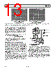
12 / 17 page  OP249 –12– REV. C SETTLING TIME Settling time is the time between when the input signal begins to change and when the output permanently enters a prescribed error band. The error bands on the output are 5 mV and 0.5 mV, respectively, for 0.1% and 0.01% accuracy. Figure 46 illustrates the OP249’s typical settling time of 870 ns. Moreover, problems in settling response, such as thermal tails and long-term ringing are nonexistent. 10 0% 100 90 500ns 10mV 870ns Figure 46. Settling Characteristics of the OP249 to 0.01% REFERENCE OR VIN VOUT 1/2 OP249 +15V –15V PM7545 DB11 - DB0 12 DATA INPUT 500 C 33pF 75 VDD 0.1 F 0.1 F OUT1 AGND VREF REFERENCE OR VIN VOUT 1/2 OP249 +15V PM7545 DB11 - DB0 12 DATA INPUT 500 C 33pF 75 VDD 0.1 F OUT1 AGND VREF VDD RFB 1/2 OP249 –15V 0.1 F R4 20k 1% R5 10k 1% R3 10k 1% 0.1 F DGND a. Unipolar Operation b. Bipolar Operation Figure 47. Fast Settling and Low Offset Error of the OP249 Enhances CMOS DAC Performance DAC OUTPUT AMPLIFIER Unity-gain stability, a low offset voltage of 300 µV typical, and a fast settling time of 870 ns to 0.01%, makes the OP249 an ideal amplifier for fast digital-to-analog converters. For CMOS DAC applications, the low offset voltage of the OP249 results in excellent linearity performance. CMOS DACs, such as the PM-7545, will typically have a code-dependent output resistance variation between 11 k Ω and 33 kΩ. The change in output resistance, in conjunction with the 11 k Ω feedback resistor, will result in a noise gain change. This causes variations in the offset error, increasing linearity errors. The OP249 features low offset voltage error, minimizing this effect and maintaining 12-bit linearity performance over the full-scale range of the converter. Since the DAC’s output capacitance appears at the operational amplifiers inputs, it is essential that the amplifier is adequately compensated. Compensation will increase the phase margin, and ensure an optimal overall settling response. The required lead compensation is achieved with Capacitor C in Figure 47. |
|
|
链接网址 |
| ALLDATASHEET是否为您带来帮助? [ DONATE ] |
关于 Alldatasheet | 广告服务 | 联系我们 | 隐私政策 | 数据表链接 | 链接交换 | 制造商名单 All Rights Reserved©Alldatasheet.com |
| Russian : Alldatasheetru.com | Korean : Alldatasheet.co.kr | Spanish : Alldatasheet.es | French : Alldatasheet.fr | Italian : Alldatasheetit.com Portuguese : Alldatasheetpt.com | Polish : Alldatasheet.pl | Vietnamese : Alldatasheet.vn Indian : Alldatasheet.in | Mexican : Alldatasheet.com.mx | British : Alldatasheet.co.uk | New Zealand : Alldatasheet.co.nz |
|
Family Site : ic2ic.com |
icmetro.com |
 Chinese ▼
 English
 Chinese
 German
 Japanese
 Russian
 Korean
 Spanish
 French
 Italian
 Portuguese
 Polish
 Vietnamese
 Indian
 Mexican
 British
 New Zealand