|
数据搜索系统,热门电子元器件搜索 |
|
|
数据搜索系统,热门电子元器件搜索 |
|
OP249ARC/883 数据表(PDF) 13 Page - Analog Devices |
|
|
|||||||||||||||||||||||||||||
OP249ARC/883 数据表(HTML) 13 Page - Analog Devices |
|
|
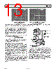
13 / 17 page  OP249 –13– REV. C Figure 48 illustrates the effect of altering the compensation on the output response of the circuit in Figure 48a. Compensation is required to address the combined effect of the DAC’s output capacitance, the op amp’s input capacitance and any stray ca- pacitance. Slight adjustments to the compensation capacitor may be required to optimize settling response for any given application . The settling time of the combination of the current output DAC and the op amp can be approximated by: tS TOTAL = (t S DAC ) 2 +(t S AMP ) 2 The actual overall settling time is affected by the noise gain of the amplifier, the applied compensation, and the equivalent input capacitance at the amplifier’s input. DISCUSSION ON DRIVING A/D CONVERTERS Settling characteristics of operational amplifiers also include an amplifier’s ability to recover, i.e., settle, from a transient current output load condition. An example of this includes an op amp driving the input from a SAR type A/D converter. Although the comparison point of the converter is usually diode clamped, the input swing of plus-and-minus a diode drop still gives rise to a significant modulation of input current. If the closed-loop out- put impedance is low enough and bandwidth of the amplifier is sufficiently large, the output will settle before the converter makes a comparison decision which will prevent linearity errors or missing codes. Figure 49 shows a settling measurement circuit for evaluating recovery from an output current transient. An output disturbing current generator provides the transient change in output load current of 1 mA. As seen in Figure 50, the OP249 has extremely fast recovery of 274 ns (to 0.01%), for a 1 mA load transient. The performance makes it an ideal amplifier for data acquisition systems. B A C = 5pF RESPONSE IS GROSSLY UNDERDAMPED, AND EXHIBITS RINGING C = 15pF FAST RISE TIME CHARACTERISTICS, BUT AT EXPENSE OF SLIGHT PEAKING IN RESPONSE Figure 48. Effect of Altering Compensation from Circuit in Figure 47a—PM7545 CMOS DAC with 1/2 OP249, Unipolar Operation. Critically Damped Response Will Be Obtained with C 33 pF |VREF| 1k IOUT = 1/2 OP249 +15V –15V 0.1 F 0.1 F +15V 1.5k 1N4148 0.1 F 220 1.8k 1k 2N3904 1k 10 F VREF 0.47 F 0.01 F * * *NOTE: DECOUPLE CLOSE TOGETHER ON GROUND PLANEWITH SHORT LEAD LENGTHS TTL INPUT +15V 2N2907 7A13 PLUG-IN 7A13 PLUG-IN 300pF Figure 49. Transient Output Impedance Test Fixture The combination of high speed and excellent dc performance of the OP249 makes it an ideal amplifier for 12-bit data acquisition systems. Examining the circuit in Figure 51, one amplifier in the OP249 provides a stable –5 V reference voltage for the VREF input of the ADC912. The other amplifier in the OP249 per- forms high speed buffering of the A/D’s input. Examining the worst case transient voltage error (Figure 52) at the Analog In node of the A/D converter: the OP249 recovers in less than 100 ns. The fast recovery is due to both the OP249’s wide bandwidth and low dc output impedance. |
|
|
链接网址 |
| ALLDATASHEET是否为您带来帮助? [ DONATE ] |
关于 Alldatasheet | 广告服务 | 联系我们 | 隐私政策 | 数据表链接 | 链接交换 | 制造商名单 All Rights Reserved©Alldatasheet.com |
| Russian : Alldatasheetru.com | Korean : Alldatasheet.co.kr | Spanish : Alldatasheet.es | French : Alldatasheet.fr | Italian : Alldatasheetit.com Portuguese : Alldatasheetpt.com | Polish : Alldatasheet.pl | Vietnamese : Alldatasheet.vn Indian : Alldatasheet.in | Mexican : Alldatasheet.com.mx | British : Alldatasheet.co.uk | New Zealand : Alldatasheet.co.nz |
|
Family Site : ic2ic.com |
icmetro.com |
 Chinese ▼
 English
 Chinese
 German
 Japanese
 Russian
 Korean
 Spanish
 French
 Italian
 Portuguese
 Polish
 Vietnamese
 Indian
 Mexican
 British
 New Zealand