|
数据搜索系统,热门电子元器件搜索 |
|
|
数据搜索系统,热门电子元器件搜索 |
|
LUCL9500AGF-D 数据表(PDF) 8 Page - Agere Systems |
|
|
|||||||||||||||||||||||||||||
LUCL9500AGF-D 数据表(HTML) 8 Page - Agere Systems |
|
|
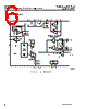
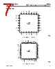
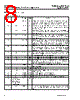
8 / 32 page  Preliminary Data Sheet September 2001 High-Voltage Ringing SLIC for VoIP Applications L9500A 8 Agere Systems Inc. Pin Information (continued) Table 1. Pin Descriptions 28-Pin PLCC 48-Pin MLCC Symbol Type Name/Function 143 NSTAT O Loop Closure Detector Output—Ring Trip Detector Output. When low, this logic output indicates that an off-hook condition exists or ringing is tripped or a ring ground has occurred. 245 VITR O Transmit ac Output Voltage. Output of internal AAC amplifier. This output is a voltage that is directly proportional to the differ- ential ac tip/ring current. 3 47 RCVP I Receive ac Signal Input (Noninverting). This high-impedance input controls to ac differential voltage on tip and ring. This node is a floating input. 4 48 RCVN I Receive ac Signal Input (Inverting). This high-impedance input controls to ac differential voltage on tip and ring. This node is a floating input. 5 1 RINGINN I Power Ring Signal Input. Couple to a sine wave or lower crest factor low-voltage ring signal. The input here is amplified to pro- vide the full power ring signal at tip and ring. This signal may be applied continuously, even during nonringing states. 6 2 RINGINP I Power Ring Signal Input. Couple to a sine wave or lower crest factor low-voltage ring signal. The input here is amplified to pro- vide the full power ring signal at tip and ring. This signal may be applied continuously, even during nonringing states. 7 6 DCOUT O dc Output Voltage. This output is a voltage that is directly pro- portional to the absolute value of the differential tip/ring current. This is used to set ring trip threshold. 88 CF2 — Filter Capacitor. Connect a capacitor from this node to ground. 910 CF1 — Filter Capacitor. Connect a capacitor from this node to CF2. 10 12 RTFLT — Ring Trip Filter. Connect this lead to DCOUT via a resistor and to AGND with a capacitor to filter the ring trip circuit to prevent spurious responses. A single-pole filter is needed. 11 13 VREF O SLIC Internal Reference Voltage. Output of internal 1.5 V ref- erence voltage. 12 15 AGND GND Analog Signal Ground. 13 16 VCC PWR Analog Power Supply. User choice of 5 V or 3.3 V nominal power or supply. 14 19 VBAT1 PWR Battery Supply 1. High-voltage battery. 15 21 VBAT2 PWR Battery Supply 2. Lower-voltage battery. 16 23 BGND GND Battery Ground. Ground return for the battery supplies. 17 3, 4, 5, 7, 9, 11, 14, 17, 18, 20, 22, 27, 29, 30, 32, 36, 37, 40, 42, 44, 46 NC — No Connection. 18 24 VPROG I Current-Limit Program Input. Connect ground to this pin to set current limit to 25 mA; leave this pin open to set current limit to 40 mA. |
|
链接网址 |
| ALLDATASHEET是否为您带来帮助? [ DONATE ] |
关于 Alldatasheet | 广告服务 | 联系我们 | 隐私政策 | 数据表链接 | 链接交换 | 制造商名单 All Rights Reserved©Alldatasheet.com |
| Russian : Alldatasheetru.com | Korean : Alldatasheet.co.kr | Spanish : Alldatasheet.es | French : Alldatasheet.fr | Italian : Alldatasheetit.com Portuguese : Alldatasheetpt.com | Polish : Alldatasheet.pl | Vietnamese : Alldatasheet.vn Indian : Alldatasheet.in | Mexican : Alldatasheet.com.mx | British : Alldatasheet.co.uk | New Zealand : Alldatasheet.co.nz |
|
Family Site : ic2ic.com |
icmetro.com |
 Chinese ▼
 English
 Chinese
 German
 Japanese
 Russian
 Korean
 Spanish
 French
 Italian
 Portuguese
 Polish
 Vietnamese
 Indian
 Mexican
 British
 New Zealand