|
数据搜索系统,热门电子元器件搜索 |
|
|
数据搜索系统,热门电子元器件搜索 |
|
LUCL9500AGF-DT 数据表(PDF) 5 Page - Agere Systems |
|
|
|||||||||||||||||||||||||||||
LUCL9500AGF-DT 数据表(HTML) 5 Page - Agere Systems |
|
|
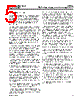
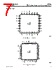
5 / 32 page  Preliminary Data Sheet September 2001 High-Voltage Ringing SLIC for VoIP Applications L9500A Agere Systems Inc. 5 Description (continued) Forward and reverse battery active modes are used for off-hook conditions. Since this device is designed for short-loop applications, the lower-voltage VBAT2 is applied during the forward and reverse active states. Battery reversal is quiet, without breaking the ac path. Rate of battery reversal may be ramped to control switching time. The magnitude of the overhead voltage in the forward and reverse active modes has a typical default value of 7.0 V, allowing for an on-hook transmission of an undis- torted signal of 3.14 dBm into 900 Ω. Additionally, this allows sufficient overhead for 500 mV of meter pulse if desired. This overhead is fixed. The ring trip detector is turned off during active modes to conserve power. Because on-hook transmission is not allowed in the scan mode, an on-hook transmission mode is defined. This mode is functionally similar to the active mode, except the tip ring voltage is derived from the higher VBAT1 rather than VBAT2. In the on-hook transmission modes with a primary bat- tery whose magnitude is greater than a nominal 51 V, the magnitude of the tip-to-ground and ring-to- ground voltage is clamped at less than 56.5 V. To minimize on-hook power, a low-power scan mode is available. In this mode, all functions except off-hook supervision are turned off to conserve power. On-hook transmission is not allowed in the scan mode. In the scan mode with a primary battery whose magni- tude is greater than a nominal 51 V, the magnitude of the tip-to-ground and ring-to-ground voltage is clamped at less than 56.5 V. A forward disconnect mode is provided, where all cir- cuits are turned off and power is denied to the loop. The device offers a ring mode, in which a power ring signal is provided to the tip/ring pair. During the ring mode, a user-supplied, low-voltage ring signal is differ- entially input to the device’s RINGIN input. This signal is amplified to produce the power ring signal. This signal may be a sine wave or filtered square wave to produce a sine wave on trapezoidal output. Ring trip detector and common-mode current detector are active during the ring mode. With maximum VBAT1 and a sine wave input, the L9500 has sufficient power to ring a 5 REN (1386 Ω + 40 µF) ringing load into 500 Ω of physical resistance. This feature eliminates the need for a separate external ring relay, associated external circuitry, and a bulk ring- ing generator. See the Applications section of this data sheet for more information. Both the ring trip and loop closure supervision func- tions are included. The loop closure has a fixed typical 10.5 mA on- to off-hook threshold in the active mode and a fixed 11.5 mA on- to off-hook threshold from the scan mode. In either case, there is a 2 mA hysteresis. The ring trip detector requires only a single-pole filter at the input, minimizing external components. The ring trip threshold at a given battery voltage is fixed. Typical ring trip threshold is 42.5 mA for a –70 V VBAT1. The device offers a ground start mode. In this mode the tip drive amplifier is turned off. The device presents a high impedance (>100 k Ω) to PT and a current limited battery (VBAT1) to PR. VBAT1 is clamped to less than 56.5 V in this mode at PR. The NSTAT loop current detctor is used for ring ground detection. In the ground start mode, since the loop current is common mode, the loop closure threshold is reduced in half, thus main- taining loop supervision at specified levels. Upon reaching the thermal shutdown temperature, the device will enter an all off mode. Upon cooling, the device will re-enter the state it was in prior to thermal shutdown. Hysteresis is built in to prevent oscillation. Data control is via a parallel unlatched control scheme. The dc current limit is fixed to either 25 mA or 40 mA depending if ground or open is applied to the VPROG current limit programming pin. Programming accuracy is ±8%. Circuitry is added to the L9500 to minimize the inrush of current from the VCC supply and to the battery supply during an on- to off-hook transition, thus saving in power supply design cost. See the Applications section of this data sheet for more information. The L9500 uses a voltage feed-current sense architec- ture; thus the transmit gain is a transconductance. The L9500 transconductance is set via a single external resistor, and this device is designed for optimal perfor- mance with a transconductance set at 300 V/A. This interface is single ended. The L9500 offers a differen- tial receive interface with a gain of 8. The L9500 is internally referenced to 1.5 V. This refer- ence voltage is output at the VREF output of the device. The SLIC output VITR is also referenced to 1.5 V. The SLIC inputs RCVP/RCVN are floating inputs. The L9500 is packaged in a 28-pin PLCC or a 48-pin MLCC package. |
|
链接网址 |
| ALLDATASHEET是否为您带来帮助? [ DONATE ] |
关于 Alldatasheet | 广告服务 | 联系我们 | 隐私政策 | 数据表链接 | 链接交换 | 制造商名单 All Rights Reserved©Alldatasheet.com |
| Russian : Alldatasheetru.com | Korean : Alldatasheet.co.kr | Spanish : Alldatasheet.es | French : Alldatasheet.fr | Italian : Alldatasheetit.com Portuguese : Alldatasheetpt.com | Polish : Alldatasheet.pl | Vietnamese : Alldatasheet.vn Indian : Alldatasheet.in | Mexican : Alldatasheet.com.mx | British : Alldatasheet.co.uk | New Zealand : Alldatasheet.co.nz |
|
Family Site : ic2ic.com |
icmetro.com |
 Chinese ▼
 English
 Chinese
 German
 Japanese
 Russian
 Korean
 Spanish
 French
 Italian
 Portuguese
 Polish
 Vietnamese
 Indian
 Mexican
 British
 New Zealand