|
数据搜索系统,热门电子元器件搜索 |
|
|
数据搜索系统,热门电子元器件搜索 |
|
AD8250ARMZ-R7 数据表(PDF) 17 Page - Analog Devices |
|
|
|||||||||||||||||||||||||||||
AD8250ARMZ-R7 数据表(HTML) 17 Page - Analog Devices |
|
|
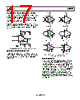
17 / 24 page  Data Sheet AD8250 Rev. C | Page 17 of 24 POWER SUPPLY REGULATION AND BYPASSING The AD8250 has high PSRR. However, for optimal performance, a stable dc voltage should be used to power the instrumentation amplifier. Noise on the supply pins can adversely affect per- formance. As in all linear circuits, bypass capacitors must be used to decouple the amplifier. Place a 0.1 μF capacitor close to each supply pin. A 10 μF tantalum capacitor can be used farther away from the part (see Figure 51) and, in most cases, it can be shared by other precision integrated circuits. AD8250 +VS +IN –IN LOAD REF 0.1µF 10µF 0.1µF 10µF –VS DGND OUT DGND A0 A1 WR Figure 51. Supply Decoupling, REF, and Output Referred to Ground INPUT BIAS CURRENT RETURN PATH The AD8250 input bias current must have a return path to its local analog ground. When the source, such as a thermocouple, cannot provide a return current path, one should be created (see Figure 52). THERMOCOUPLE +VS REF –VS AD8250 CAPACITIVELY COUPLED +VS REF C C –VS AD8250 TRANSFORMER +VS REF –VS AD8250 INCORRECT CAPACITIVELY COUPLED +VS REF C R R C –VS AD8250 1 fHIGH-PASS = 2πRC THERMOCOUPLE +VS REF –VS 10MΩ AD8250 TRANSFORMER +VS REF –VS AD8250 CORRECT Figure 52. Creating an IBIAS Return Path INPUT PROTECTION All terminals of the AD8250 are protected against ESD. Note that 2.2 kΩ series resistors precede the ESD diodes as shown in Figure 47. The resistors limit current into the diodes and allow for dc overload conditions 13 V above the positive supply and 13 V below the negative supply. An external resistor should be used in series with each input to limit current for voltages greater than 13 V beyond either supply rail. In either scenario, the AD8250 safely handles a continuous 6 mA current at room temperature. For applications where the AD8250 encounters extreme overload voltages, external series resistors and low leakage diode clamps, such as BAV199Ls, FJH1100s, or SP720s, should be used. |
|
|
链接网址 |
| ALLDATASHEET是否为您带来帮助? [ DONATE ] |
关于 Alldatasheet | 广告服务 | 联系我们 | 隐私政策 | 数据表链接 | 链接交换 | 制造商名单 All Rights Reserved©Alldatasheet.com |
| Russian : Alldatasheetru.com | Korean : Alldatasheet.co.kr | Spanish : Alldatasheet.es | French : Alldatasheet.fr | Italian : Alldatasheetit.com Portuguese : Alldatasheetpt.com | Polish : Alldatasheet.pl | Vietnamese : Alldatasheet.vn Indian : Alldatasheet.in | Mexican : Alldatasheet.com.mx | British : Alldatasheet.co.uk | New Zealand : Alldatasheet.co.nz |
|
Family Site : ic2ic.com |
icmetro.com |
 Chinese ▼
 English
 Chinese
 German
 Japanese
 Russian
 Korean
 Spanish
 French
 Italian
 Portuguese
 Polish
 Vietnamese
 Indian
 Mexican
 British
 New Zealand