|
数据搜索系统,热门电子元器件搜索 |
|
|
数据搜索系统,热门电子元器件搜索 |
|
TLV2211CDBVT 数据表(PDF) 25 Page - Texas Instruments |
|
|
|
|||||||||||||||||||||||||||||
TLV2211CDBVT 数据表(HTML) 25 Page - Texas Instruments |
|
|
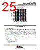
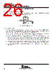
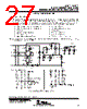
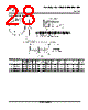
25 / 31 page  SLOS156E − MAY 1996 − REVISED SEPTEMBER 2006 TLV2211, TLV2211Y Advanced LinCMOS RAILTORAIL MICROPOWER SINGLE OPERATIONAL AMPLIFIERS 25 POST OFFICE BOX 655303 • DALLAS, TEXAS 75265 TYPICAL CHARACTERISTICS UNITY-GAIN BANDWIDTH vs LOAD CAPACITANCE CL − Load Capacitance − pF 60 10 40 0 80 50 70 20 30 101 10 2 10 3 10 4 10 5 TA = 25°C 10 6 Figure 53 APPLICATION INFORMATION driving large capacitive loads The TLV2211 is designed to drive larger capacitive loads than most CMOS operational amplifiers. Figures 51 and 52 illustrate its ability to drive loads up to 600 pF while maintaining good gain and phase margins (Rnull = 0). A smaller series resistor (Rnull) at the output of the device (see Figure 54) improves the gain and phase margins when driving large capacitive loads. Figures 51 and 52 show the effects of adding series resistances of 500 Ω and 1000 Ω. The addition of this series resistor has two effects: the first is that it adds a zero to the transfer function and the second is that it reduces the frequency of the pole associated with the output load in the transfer function. The zero introduced to the transfer function is equal to the series resistance times the load capacitance. To calculate the improvement in phase margin, equation 1 can be used. ∆φ m1 + tan –1 2 ×π × UGBW × R null × C L ∆φ m1 + improvement in phase margin UGBW + unity-gain bandwidth frequency R null + output series resistance C L + load capacitance (1) Where : |
|
链接网址 |
| ALLDATASHEET是否为您带来帮助? [ DONATE ] |
关于 Alldatasheet | 广告服务 | 联系我们 | 隐私政策 | 数据表链接 | 链接交换 | 制造商名单 All Rights Reserved©Alldatasheet.com |
| Russian : Alldatasheetru.com | Korean : Alldatasheet.co.kr | Spanish : Alldatasheet.es | French : Alldatasheet.fr | Italian : Alldatasheetit.com Portuguese : Alldatasheetpt.com | Polish : Alldatasheet.pl | Vietnamese : Alldatasheet.vn Indian : Alldatasheet.in | Mexican : Alldatasheet.com.mx | British : Alldatasheet.co.uk | New Zealand : Alldatasheet.co.nz |
|
Family Site : ic2ic.com |
icmetro.com |
 Chinese ▼
 English
 Chinese
 German
 Japanese
 Russian
 Korean
 Spanish
 French
 Italian
 Portuguese
 Polish
 Vietnamese
 Indian
 Mexican
 British
 New Zealand