|
数据搜索系统,热门电子元器件搜索 |
|
|
数据搜索系统,热门电子元器件搜索 |
|
AD8065WARTZ-R7 数据表(PDF) 25 Page - Analog Devices |
|
|
|||||||||||||||||||||||||||||
AD8065WARTZ-R7 数据表(HTML) 25 Page - Analog Devices |
|
|
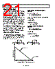
25 / 29 page  AD8065/AD8066 Rev. J | Page 24 of 28 RSH = 1011Ω VO RF CF CM RF CM CD CF +CS CS VB IPHOTO Figure 58. Wideband Photodiode Preamp INPUT-TO-OUTPUT COUPLING To minimize capacitive coupling between the inputs and output, the output signal traces should not be parallel with the inputs. WIDEBAND PHOTODIODE PREAMP Figure 58 shows an I/V converter with an electrical model of a photodiode. The basic transfer function is F F F PHOTO OUT R sC R I V + × = 1 where IPHOTO is the output current of the photodiode, and the parallel combination of RF and CF sets the signal bandwidth. The stable bandwidth attainable with this preamp is a function of RF, the gain bandwidth product of the amplifier, and the total capacitance at the amplifier’s summing junction, including CS and the amplifier input capacitance. RF and the total capacitance produce a pole in the amplifier’s loop transmission that can result in peaking and instability. Adding CF creates a 0 in the loop transmission that compensates for the pole’s effect and reduces the signal bandwidth. It can be shown that the signal bandwidth resulting in a 45° phase margin (f(45)) is defined by () S F CR C R f f × × π = 2 45 where fCR is the amplifier crossover frequency, RF is the feedback resistor, and CS is the total capacitance at the amplifier summing junction (amplifier + photodiode + board parasitics). The value of CF that produces f(45) can be shown to be CR F S F f R C C × × π = 2 The frequency response in this case shows about 2 dB of peaking and 15% overshoot. Doubling CF and cutting the bandwidth in half results in a flat frequency response with about 5% transient overshoot. The preamp’s output noise over frequency is shown in Figure 59. FREQUENCY (Hz) 2 πRFCF 2 πRF (CF +CS +CM +2CD) (CS +CM +2CD +CF)/CF RF NOISE VEN (CF +CS +CM + 2CD)/CF f3 f2 f3 = VEN f1 f2 = f1 = 1 1 fCR NOISE DUE TO AMPLIFIER Figure 59. Photodiode Voltage Noise Contributions The pole in the loop transmission translates to a 0 in the amplifier’s noise gain, leading to an amplification of the input voltage noise over frequency. The loop transmission 0 introduced by CF limits the amplification. The noise gain bandwidth extends past the preamp signal bandwidth and is eventually rolled off by the decreasing loop gain of the amplifier. Keeping the input terminal impedances matched is recommended to eliminate common-mode noise peaking effects, which adds to the output noise. Integrating the square of the output voltage noise spectral density over frequency and then taking the square root allows users to obtain the total rms output noise of the preamp. Table 5 summarizes approximations for the amplifier and feedback and source resistances. Noise components for an example preamp with RF = 50 kΩ, CS = 15 pF, and CF = 2 pF (bandwidth of about 1.6 MHz) are also listed. |
|
|
链接网址 |
| ALLDATASHEET是否为您带来帮助? [ DONATE ] |
关于 Alldatasheet | 广告服务 | 联系我们 | 隐私政策 | 数据表链接 | 链接交换 | 制造商名单 All Rights Reserved©Alldatasheet.com |
| Russian : Alldatasheetru.com | Korean : Alldatasheet.co.kr | Spanish : Alldatasheet.es | French : Alldatasheet.fr | Italian : Alldatasheetit.com Portuguese : Alldatasheetpt.com | Polish : Alldatasheet.pl | Vietnamese : Alldatasheet.vn Indian : Alldatasheet.in | Mexican : Alldatasheet.com.mx | British : Alldatasheet.co.uk | New Zealand : Alldatasheet.co.nz |
|
Family Site : ic2ic.com |
icmetro.com |
 Chinese ▼
 English
 Chinese
 German
 Japanese
 Russian
 Korean
 Spanish
 French
 Italian
 Portuguese
 Polish
 Vietnamese
 Indian
 Mexican
 British
 New Zealand