|
数据搜索系统,热门电子元器件搜索 |
|
|
数据搜索系统,热门电子元器件搜索 |
|
AD8210YR-R7 数据表(PDF) 10 Page - Analog Devices |
|
|
|||||||||||||||||||||||||||||
AD8210YR-R7 数据表(HTML) 10 Page - Analog Devices |
|
|
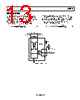
10 / 16 page  AD8210 Data Sheet Rev. D | Page 10 of 16 THEORY OF OPERATION In typical applications, the AD8210 amplifies a small differential input voltage generated by the load current flowing through a shunt resistor. The AD8210 rejects high common-mode voltages (up to 65 V) and provides a ground referenced buffered output that interfaces with an analog-to-digital converter (ADC). Figure 26 shows a simplified schematic of the AD8210. The AD8210 is comprised of two main blocks, a differential amplifier and an instrumentation amplifier. A load current flowing through the external shunt resistor produces a voltage at the input terminals of the AD8210. The input terminals are connected to the differential amplifier (A1) by R1 and R2. A1 nulls the voltage appearing across its own input terminals by adjusting the current through R1 and R2 with Q1 and Q2. When the input signal to the AD8210 is 0 V, the currents in R1 and R2 are equal. When the differential signal is nonzero, the current increases through one of the resistors and decreases in the other. The current difference is proportional to the size and polarity of the input signal. The differential currents through Q1 and Q2 are converted into a differential voltage by R3 and R4. A2 is configured as an instrumentation amplifier. The differential voltage is converted into a single-ended output voltage by A2. The gain is internally set with precision-trimmed, thin film resistors to 20 V/V. The output reference voltage is easily adjusted by the VREF1 pin and the VREF2 pin. In a typical configuration, VREF1 is connected to VCC while VREF2 is connected to GND. In this case, the output is centered at VCC/2 when the input signal is 0 V. ISHUNT RSHUNT AD8210 VOUT = (ISHUNT × RSHUNT) × 20 A2 R1 R2 VS VREF1 VREF2 GND A1 R3 R4 Q1 Q2 Figure 26. Simplified Schematic |
|
|
链接网址 |
| ALLDATASHEET是否为您带来帮助? [ DONATE ] |
关于 Alldatasheet | 广告服务 | 联系我们 | 隐私政策 | 数据表链接 | 链接交换 | 制造商名单 All Rights Reserved©Alldatasheet.com |
| Russian : Alldatasheetru.com | Korean : Alldatasheet.co.kr | Spanish : Alldatasheet.es | French : Alldatasheet.fr | Italian : Alldatasheetit.com Portuguese : Alldatasheetpt.com | Polish : Alldatasheet.pl | Vietnamese : Alldatasheet.vn Indian : Alldatasheet.in | Mexican : Alldatasheet.com.mx | British : Alldatasheet.co.uk | New Zealand : Alldatasheet.co.nz |
|
Family Site : ic2ic.com |
icmetro.com |
 Chinese ▼
 English
 Chinese
 German
 Japanese
 Russian
 Korean
 Spanish
 French
 Italian
 Portuguese
 Polish
 Vietnamese
 Indian
 Mexican
 British
 New Zealand