|
数据搜索系统,热门电子元器件搜索 |
|
|
数据搜索系统,热门电子元器件搜索 |
|
AD8051ARTZ-R2 数据表(PDF) 20 Page - Analog Devices |
|
|
|||||||||||||||||||||||||||||
AD8051ARTZ-R2 数据表(HTML) 20 Page - Analog Devices |
|
|
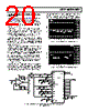
20 / 25 page  AD8051/AD8052/AD8054 Rev. J | Page 19 of 24 ANALOG-TO-DIGITAL AND DIGITAL-TO-ANALOG APPLICATIONS Figure 50 is a schematic showing the AD8051 used as a driver for an AD9201, a 10-bit, 20 MSPS, dual analog-to-digital converter. This converter is designed to convert I and Q signals in communications systems. In this application, only the I channel is being driven. The I channel is enabled by applying a logic high to SELECT (Pin 13). The AD8051 is running from a dual supply and is configured for a gain of +2. The input signal is terminated in 50 Ω and the output is 2 V p-p, which is the maximum input range of the AD9201. The 22 Ω series resistor limits the maximum current that flows and helps to lower the distortion of the ADC. The AD9201 has differential inputs for each channel. These are designated the A and B inputs. The B inputs of each channel are connected to VREF (Pin 22), which supplies a positive reference of 2.5 V. Each of the B inputs has a small low-pass filter that also helps to reduce distortion. The output of the op amp is ac-coupled into INA-I (Pin 16) via two parallel capacitors to provide good high frequency and low frequency coupling. The 1 kΩ resistor references the signal to VREF that is applied to INB-I. Thus, INA-I swings both positive and negative with respect to the bias voltage applied to INB-I. With the sampling clock running at 20 MSPS, the analog-to- digital output was analyzed with a digital analyzer. Two input frequencies were used, 1 MHz and 9.5 MHz, which is just short of the Nyquist frequency. These signals were well filtered to minimize any harmonics. Figure 48 shows the FFT response of the ADC for the case of a 1 MHz analog input. The SFDR is 71.66 dB, and the analog-to- digital is producing 8.8 ENOB (effective number of bits). When the analog frequency was raised to 9.5 MHz, the SFDR was reduced to −60.18 dB and the ADC operated with 8.46 ENOBs as shown in Figure 49. The inclusion of the AD8051 in the circuit did not worsen the distortion performance of the AD9201. PART# 0 FCLK FUND VIN THD SNR SINAD ENOB SFDR 2ND 3RD 4TH 5TH 6TH 7TH 8TH 9TH FFTSIZE 8192 20.0MHz 998.5kHz –0.51dB –68.13 54.97 54.76 8.80 71.66 –74.53 –76.06 –76.35 –79.05 –80.36 –75.08 –88.12 –77.87 10 0 –10 –20 –30 –40 –50 –60 –70 –80 –90 –100 –110 –120 FREQUENCY (MHz) 0 1 2 3 45 67 8 9 10 FUND 2ND 5TH 6TH 7TH 8TH 9TH 4TH 3RD Figure 48. FFT Plot for AD8051 Driving the AD9201 at 1 MHz PART# 0 FCLK FUND VIN THD SNR SINAD ENOB SFDR 2ND 3RD 4TH 5TH 6TH 7TH 8TH 9TH FFTSIZE 8192 20.0MHz 9.5MHz –0.44dB –57.08 54.65 52.69 8.46 60.18 –60.18 –60.23 –82.01 –78.83 –81.28 –77.28 –84.54 –92.78 10 0 –10 –20 –30 –40 –50 –60 –70 –80 –90 –100 –110 –120 FREQUENCY (MHz) 0 1 2 3 45 67 8 9 10 FUND 2ND 5TH 6TH 7TH 8TH 4TH 3RD Figure 49. FFT Plot for AD8051 Driving the AD9201 at 9.5 MHz AD8051 +5V VREF AVDD SELECT INA-I 10pF CLOCK SLEEP D9 D1 D2 D3 D4 D5 D6 D7 D0 DVDD AVSS REFSENSE AD9201 DVSS CHIP–SELECT INB-I REFT-I REFB-I REFB-Q REFT-Q INB-Q INA-Q D8 DATA OUT 10pF –5V 10pF 10pF 15 16 17 18 19 20 21 22 23 24 25 26 27 28 14 13 12 11 10 9 8 7 6 5 4 3 2 1 0.1µF 10µF +5V +VDD 10µF 0.1µF 0.1µF 0.1µF 10µF 0.1µF 10µF 0.1µF 10µF 0.1µF 0.1µF 0.1µF +5V 22Ω 22Ω 22Ω 22Ω 22Ω 1kΩ 1kΩ 0.33µF 0.01µF 1kΩ 10µF 0.1µF 10µF 0.1µF 50Ω 3 2 7 4 6 Figure 50. The AD8051 Driving an AD9201, a 10-Bit, 20 MSPS Analog-to-Digital Converter |
|
|
链接网址 |
| ALLDATASHEET是否为您带来帮助? [ DONATE ] |
关于 Alldatasheet | 广告服务 | 联系我们 | 隐私政策 | 数据表链接 | 链接交换 | 制造商名单 All Rights Reserved©Alldatasheet.com |
| Russian : Alldatasheetru.com | Korean : Alldatasheet.co.kr | Spanish : Alldatasheet.es | French : Alldatasheet.fr | Italian : Alldatasheetit.com Portuguese : Alldatasheetpt.com | Polish : Alldatasheet.pl | Vietnamese : Alldatasheet.vn Indian : Alldatasheet.in | Mexican : Alldatasheet.com.mx | British : Alldatasheet.co.uk | New Zealand : Alldatasheet.co.nz |
|
Family Site : ic2ic.com |
icmetro.com |
 Chinese ▼
 English
 Chinese
 German
 Japanese
 Russian
 Korean
 Spanish
 French
 Italian
 Portuguese
 Polish
 Vietnamese
 Indian
 Mexican
 British
 New Zealand