|
数据搜索系统,热门电子元器件搜索 |
|
|
数据搜索系统,热门电子元器件搜索 |
|
AD8305ACP-R2 数据表(PDF) 19 Page - Analog Devices |
|
|
|||||||||||||||||||||||||||||
AD8305ACP-R2 数据表(HTML) 19 Page - Analog Devices |
|
|
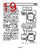
19 / 24 page  AD8305 Rev. B | Page 19 of 24 CHARACTERIZATION METHODS During the characterization of the AD8305, the device was treated as a precision current-input logarithmic converter, because it is not practical for several reasons to generate accurate photocurrents by illuminating a photodiode. The test currents are generated by using well calibrated current sources, such as the Keithley 236, or by using a high value resistor from a voltage source to the input pin. Great care is needed when using very small input currents. For example, the triax output connection from the current generator was used with the guard tied to VSUM. The input trace on the PC board was guarded by connecting adjacent traces to VSUM. These measures are needed to minimize the risk of leakage current paths. With 0.5 V as the nominal bias on the INPT pin, a leakage-path resistance of 1 GΩ to ground would subtract 0.5 nA from the input, which amounts to an error of −0.44 dB for a source current of 10 nA. Additionally, the very high output resistance at the input pins and the long cables commonly needed during characterization allow 60 Hz and RF emissions to introduce substantial measurement errors. Careful guarding techniques are essential to reduce the pickup of these spurious signals. VSUM VNEG VREF IREF INPT VOUT BFIN VLOG TRIAX CONNECTORS (SIGNAL – INPT AND IREF GUARD – VSUM SHIELD – GROUND) AD8305 CHARACTERIZATION BOARD KEITHLEY 236 KEITHLEY 236 DC MATRIX/DC SUPPLIES/DMM VPOS Figure 42. Primary Characterization Setup The primary characterization setup shown in Figure 42 is used to measure VREF, the static (dc) performance, logarithmic conformance, slope and intercept, the voltages appearing at pins VSUM, INPT and IREF, and the buffer offset and VREF drift with temperature. To ensure stable operation over the full current range of IREF and temperature extremes, filter components of C1 = 4.7 nF and R13 = 2 kΩ are used at pin to IREF ground. In some cases, a fixed resistor between pins VREF and IREF was used in place of a precision current source. For the dynamic tests, including noise and bandwidth measurements, more specialized setups are required. AD8305 12 11 10 9 57 8 COMM COMM COMM COMM 16 13 14 15 1 2 3 4 VSUM VRDZ VREF IREF INPT VOUT SCAL BFIN VLOG 0.1µF OUTPUT AD8138 EVALUATION BOARD A B +IN BNC-T INPUT R INPUT A INPUT B HP 3577A NETWORK ANALYZER +VS AD8138 PROVIDES DC OFFSET VNEG VNEG VPOS 6 Figure 43. Configuration for Buffer Amplifier Bandwidth Measurement Figure 43 shows the configuration used to measure the buffer amplifier bandwidth. The AD8138 evaluation board includes provisions to offset VLOG at the buffer input, allowing measurements over the full range of IPD using a single supply. The network analyzer input impedances were set to 1 MΩ. 0.1µF OUTPUT AD8138 EVALUATION BOARD A B +IN INPUT B INPUT A INPUT R HP 3577A NETWORK ANALYZER +VS POWER SPLITTER 1nF 1kΩ 1kΩ 1nF R1 R2 AD8305 12 11 10 9 1 2 3 4 57 8 COMM COMM COMM COMM 16 13 14 15 VSUM VRDZ VREF IREF INPT VOUT SCAL BFIN VLOG VNEG VNEG VPOS 6 Figure 44. Configuration for Logarithmic Amplifier Bandwidth Measurement |
|
|
链接网址 |
| ALLDATASHEET是否为您带来帮助? [ DONATE ] |
关于 Alldatasheet | 广告服务 | 联系我们 | 隐私政策 | 数据表链接 | 链接交换 | 制造商名单 All Rights Reserved©Alldatasheet.com |
| Russian : Alldatasheetru.com | Korean : Alldatasheet.co.kr | Spanish : Alldatasheet.es | French : Alldatasheet.fr | Italian : Alldatasheetit.com Portuguese : Alldatasheetpt.com | Polish : Alldatasheet.pl | Vietnamese : Alldatasheet.vn Indian : Alldatasheet.in | Mexican : Alldatasheet.com.mx | British : Alldatasheet.co.uk | New Zealand : Alldatasheet.co.nz |
|
Family Site : ic2ic.com |
icmetro.com |
 Chinese ▼
 English
 Chinese
 German
 Japanese
 Russian
 Korean
 Spanish
 French
 Italian
 Portuguese
 Polish
 Vietnamese
 Indian
 Mexican
 British
 New Zealand