|
数据搜索系统,热门电子元器件搜索 |
|
|
数据搜索系统,热门电子元器件搜索 |
|
M35072-059FP 数据表(PDF) 11 Page - Mitsubishi Electric Semiconductor |
|
|
|||||||||||||||||||||||||||||
M35072-059FP 数据表(HTML) 11 Page - Mitsubishi Electric Semiconductor |
|
|
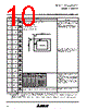
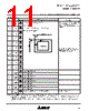
11 / 52 page  MITSUBISHI MICROCOMPUTERS M35072-XXXFP SCREEN CHARACTER and PATTERN DISPLAY CONTROLLERS 11 (4) Address 12316 The vertical start location is specified using the 10 bits from VP9 to VP0. VP9 to VP0 = (00000000002) setting is forbidden. HS* (shown left) shows horizontal __ display start location that is register B/F (address 12816) = 0 is set. 0 1 0 1 0 1 0 1 0 1 0 1 0 1 0 1 0 1 0 1 0 1 0 1 0 1 0 1 0 1 0 1 2 3 4 5 6 7 8 9 A B C D E VP0 VP1 VP2 VP3 VP4 VP5 VP6 VP7 VP8 VP9 TEST0 TEST1 TEST2 TEST3 EXCK1 If VS is the vertical display start location, VS = H × 2nVPn H: Cycle with the horizontal synchronizing pulse 1023 settings are possible. 9 Σ n = 0 It should be fixed to "0". Can not be used. It should be fixed to "0". Can not be used. It should be fixed to "0". Can not be used. It should be fixed to "0". Can not be used. For setting, see Register EXCK0 (address 12016). Display clock setting Register DA Function Contents Remarks Status (Note 3) ____ Notes 1. The mark around the status value means the reset status by the "L" level is input to AC pin. 2. The page in which data is written is controlled by the DAF bit. When set to "0", data is written into page 0, whereas when set to "1", data is written into page 1. 3. Registers marked with (Note 3) are found only in page 0, therefore the register value does not change when the DAF bit is set to "1". (Note 3) (Note 3) (Note 3) (Note 3) Display area HS * VS HOR |
|
链接网址 |
| ALLDATASHEET是否为您带来帮助? [ DONATE ] |
关于 Alldatasheet | 广告服务 | 联系我们 | 隐私政策 | 数据表链接 | 链接交换 | 制造商名单 All Rights Reserved©Alldatasheet.com |
| Russian : Alldatasheetru.com | Korean : Alldatasheet.co.kr | Spanish : Alldatasheet.es | French : Alldatasheet.fr | Italian : Alldatasheetit.com Portuguese : Alldatasheetpt.com | Polish : Alldatasheet.pl | Vietnamese : Alldatasheet.vn Indian : Alldatasheet.in | Mexican : Alldatasheet.com.mx | British : Alldatasheet.co.uk | New Zealand : Alldatasheet.co.nz |
|
Family Site : ic2ic.com |
icmetro.com |
 Chinese ▼
 English
 Chinese
 German
 Japanese
 Russian
 Korean
 Spanish
 French
 Italian
 Portuguese
 Polish
 Vietnamese
 Indian
 Mexican
 British
 New Zealand