|
数据搜索系统,热门电子元器件搜索 |
|
|
数据搜索系统,热门电子元器件搜索 |
|
IX2204NETR 数据表(PDF) 7 Page - IXYS Corporation |
|
|
|||||||||||||||||||||||||||||
IX2204NETR 数据表(HTML) 7 Page - IXYS Corporation |
|
|
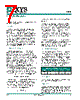
7 / 10 page  INTEGRATED CIRCUITS DIVISION IX2204 R03 www.ixysic.com 7 3 Functional Description 3.1 Input The INA and INB inputs are TTL compatible and must be referenced to GND. 3.2 Mode The MODE input determines how the desaturation protection and Under-Voltage Lock Out (UVLO) protection circuitry controls the OUTHA, OUTLA, OUTHB and OUTLB outputs. For parallel-mode IGBT drive, MODE should be connected to GND (see 4.1). For driving IGBTs that require higher gate drive current than the IX2204 can provide, the IX2204 can be used to control external drive transistors. In this stacked configuration, the external drive transistors constitute an inverting stage, and MODE should be connected to VHA for proper desaturation protection and UVLO operation (see 4.3). 3.3 Desaturation Protection The desaturation protection circuit ensures the protection of an external IGBT in the event of an over-current situation. When the voltage at DESAT exceeds 1.4V (typically) and MODE is connected to GND, OUTLA and OUTLB are driven low in a two-step process. First OUTLA, OUTHA, OUTLB and OUTHB are all turned off (high impedance). Then after a programmable time (tTRISTATE), both OUTLA and OUTLB are turned on (driven low), which quickly turns off the IGBT. This two-step action avoids both dangerous over-voltages across the IGBT and reverse-bias SOA problems, especially during a short circuit turn-off. The time that all the outputs are in tristate is set by an internal current source and an external capacitor (CTRISTATE ) that is connected to the TRISTATE pin. The tristate time is approximately: tTRISTATE = 8750 • CTRISTATE The desaturation circuit is disabled for a fixed blanking time to avoid detecting a false desaturation event during IGBT turn-on, thus allowing enough time for IGBT saturation. This blanking time is set by an internal current source and an external capacitor, CBLK. The blanking time is approximately: tBLK = 8750 • CBLK This blanking time starts when INA transitions from low to high. The desaturation two-step turn off is slightly different when MODE is connected to VHA for stack-mode IGBT drive. When the DESAT voltage exceeds 1.4V, OUTHA and OUTLB are turned on, tristating the IGBT. After the tTRISTATE time, OUTHA and OUTLB are turned off, and OUTHB is turned on, which in conjunction with the external drive transistor quickly turns off the IGBT. When MODE is connected to VHA, the blanking time starts when INA transitions from high to low. The desaturation protection circuit cannot be used when the IX2204 is used to drive two separate IGBTs (direct IGBT drive, see 4.2). When driving two separate IGBTs, the DESAT, TRISTATE, MODE, and BLANK pins should all be connected to GND. 3.4 Under-Voltage Protection The Under Voltage Lock Out (UVLO) circuit protects the IGBT from insufficient gate voltage. The UVLO circuit monitors the VHA supply voltage. If MODE is connected to GND and VHA is below the UVLO+ threshold, OUTHA and OUTHB are both turned-off (high impedance), and both OUTLA and OUTLB are both turned on (pulled low). If VHA is below the UVLO+ threshold and MODE is connected to VHA, OUTHA and OUTHB are both are turned on, and OUTLA and OUTLB are both turned off. 3.5 Fault Output The FAULT output is pulled low during a desaturation event, or when VHA is below UVLO+. 3.6 Outputs The output stages are able to source 2A, and sink 4A. Separated sink and source outputs allow independent gate charge and discharge control. For higher gate drive applications, the source and sink outputs can be paralleled to source 4A, and sink 8A. Table 2: Output States with VHA < UVLO+ Mode OUTHA OUTLA OUTHB OUTLB GNDZ 0Z0 VHA 1 Z1Z |
|
|
链接网址 |
| ALLDATASHEET是否为您带来帮助? [ DONATE ] |
关于 Alldatasheet | 广告服务 | 联系我们 | 隐私政策 | 数据表链接 | 链接交换 | 制造商名单 All Rights Reserved©Alldatasheet.com |
| Russian : Alldatasheetru.com | Korean : Alldatasheet.co.kr | Spanish : Alldatasheet.es | French : Alldatasheet.fr | Italian : Alldatasheetit.com Portuguese : Alldatasheetpt.com | Polish : Alldatasheet.pl | Vietnamese : Alldatasheet.vn Indian : Alldatasheet.in | Mexican : Alldatasheet.com.mx | British : Alldatasheet.co.uk | New Zealand : Alldatasheet.co.nz |
|
Family Site : ic2ic.com |
icmetro.com |
 Chinese ▼
 English
 Chinese
 German
 Japanese
 Russian
 Korean
 Spanish
 French
 Italian
 Portuguese
 Polish
 Vietnamese
 Indian
 Mexican
 British
 New Zealand