|
数据搜索系统,热门电子元器件搜索 |
|
|
数据搜索系统,热门电子元器件搜索 |
|
PL138-48OC-R 数据表(PDF) 12 Page - Microchip Technology |
|
|
|||||||||||||||||||||||||||||
PL138-48OC-R 数据表(HTML) 12 Page - Microchip Technology |
|
|
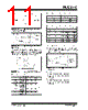
12 / 20 page  PL138-48 DS20005543B-page 12 2016 Microchip Technology Inc. FIGURE 5-12: LVPECL Termination Schematic #2. Schematic #2 is an alternative simplified termination. •VCC = 3.3V - Ideal value: RT = 48.7Ω - Commercial value: RT = 50Ω (E24: 51Ω) •VCC = 2.5V - Ideal value: RT = 18.7Ω - Commercial value: RT = 18Ω 5.3 Power Considerations Driving LVPECL outputs requires an amount of power that can warm up the chip significantly. The general requirement for the chip is that the junction temperature should not exceed +110°C. The power consumption can be divided into two parts: 1. Core power dissipation 2. Output buffer power dissipation 5.3.1 CORE POWER DISSIPATION The chip core power is equal to VCC × IEE. With a worst case VCC and IEE, the power dissipation in the core is 3.63V × 45 mA = 163 mW. 5.3.2 OUTPUT BUFFER POWER DISSIPATION The output buffers are not exposed to the full VCC – VEE voltage. On the differential output, one line is at logic 1 with a small voltage across the buffer and a large output current. The other line is at logic 0 with a larger voltage across the buffer and a smaller output current. The power dissipation per output buffer is 32 mW. Only buffers that are loaded will have power dissipation. With all 4 buffers loaded the worst case output buffer power dissipation will be 128 mW. Total chip power dissipation, worst case, is 163 mW + 128 mW = 291 mW. 5.3.3 JUNCTION TEMPERATURE How much the chip is warmed up from the power dissipation depends upon the thermal resistance from the chip to the environment, also known as “junction to ambient”. The thermal resistance depends upon the type of package, how the package is assembled to the PCB and if there is additional air flow for improved cooling. The temperature of the chip (junction) will be higher than the environment (ambient) with an amount equal to θJA × Power. For an ambient temperature of +85°C, all outputs loaded and no air flow, the junction temperature TJ = 85°C + 73 × 0.291 = 106°C. The temperature of the chip (junction) will be higher than the environment (ambient) with an amount equal to θJA × Power. For an ambient temperature of +85°C, all outputs loaded and no air flow, the junction temperature TJ = 85°C + 60 × 0.291 = 102°C. TABLE 5-4: 20-PIN TSSOP THERMAL RESISTANCE Air Flow Velocity in Linear Feet/Minute θJA Value for JEDEC Standard Multi-Layer PCB 073°C/W 200 67°C/W 500 64°C/W TABLE 5-5: 16-PIN QFN THERMAL RESISTANCE Air Flow Velocity in Linear Feet/Minute θJA Value for JEDEC Standard Multi-Layer PCB 060°C/W 200 53°C/W 500 46°C/W |
|
|
链接网址 |
| ALLDATASHEET是否为您带来帮助? [ DONATE ] |
关于 Alldatasheet | 广告服务 | 联系我们 | 隐私政策 | 数据表链接 | 链接交换 | 制造商名单 All Rights Reserved©Alldatasheet.com |
| Russian : Alldatasheetru.com | Korean : Alldatasheet.co.kr | Spanish : Alldatasheet.es | French : Alldatasheet.fr | Italian : Alldatasheetit.com Portuguese : Alldatasheetpt.com | Polish : Alldatasheet.pl | Vietnamese : Alldatasheet.vn Indian : Alldatasheet.in | Mexican : Alldatasheet.com.mx | British : Alldatasheet.co.uk | New Zealand : Alldatasheet.co.nz |
|
Family Site : ic2ic.com |
icmetro.com |
 Chinese ▼
 English
 Chinese
 German
 Japanese
 Russian
 Korean
 Spanish
 French
 Italian
 Portuguese
 Polish
 Vietnamese
 Indian
 Mexican
 British
 New Zealand