|
数据搜索系统,热门电子元器件搜索 |
|
|
数据搜索系统,热门电子元器件搜索 |
|
MSW2000-200-R 数据表(PDF) 11 Page - M/A-COM Technology Solutions, Inc. |
|
|
|||||||||||||||||||||||||||||
MSW2000-200-R 数据表(HTML) 11 Page - M/A-COM Technology Solutions, Inc. |
|
|
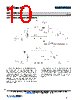
11 / 15 page  SP2T PIN Diode Switch Rev. V1 MSW200x-200 11 11 M/A-COM Technology Solutions Inc. (MACOM) and its affiliates reserve the right to make changes to the product(s) or information contained herein without notice. Visit www.macom.com for additional data sheets and product information. For further information and support please visit: https://www.macom.com/support DS-xxxxxxx 11 Transmit State In the TX state, the series PIN diode between the ANT and TX ports is forward biased by applying 0 V to the TX bias input port (pin 1 of multi-pin connector P1). The magnitude of the resultant bias current through the diode is primarily determined by the voltage applied to the ANT bias port (pin 3 of J1), the magnitude of the forward voltage across the PIN diode and the resistance of R1. This current is nominally 100 mA. At the same time, the PIN diode connected between RX and DC ports is also forward biased by applying a higher bias voltage, nominally 28 V, to the RX bias port (pin 7 of P1) and 0 V to the DC bias port (pin 5 of P1). Under this condition, the PIN diode connected between the ANT and RX port is reverse biased and the PIN diode connected between the RX and DC ports is forward biased. The magnitude of the bias current through this diode is primarily determined by the voltage applied to the RX bias port, the magnitude of the forward voltage across the PIN diode and the resistance of R2. This current is nominally 25 mA. The RX series PIN diode, which is connected between the ANT and RX ports, must be reverse biased during the transmit state. The reverse bias voltage must be sufficiently large to maintain the diode in its non-conducting, high impedance state when large RF signal voltage may be present in the ANT-to-TX path. The reverse voltage across this diode is the arithmetic difference of the bias voltage applied to the RX bias port and the DC forward voltage of the forward-biased transmit series PIN diode. The minimum voltage required to maintain the series diode on the RX side of the switch out of conduction is a function of the magnitude of the RF voltage present, the standing wave present at the RX series diode’s anode, the frequency of the RF signal and the characteristics of the RX series diode, among other factors. Minimum control voltages for several signal frequencies are shown in the table “Minimum Reverse Bias Voltage”, assuming the input power to the RX or ANT port to be 100 W CW and the VSWR on the ANT-TX path to be 1.5:1. It is important to note that the evaluation board, as supplied from the factory, is not capable of handling RF input signals larger than 45 dBm. If performance of the switch under larger input signals is to be evaluated, an adequate heat sink must be properly attached to the evaluation board, and several of the passive components on the board must be changed in order to safely handle the dissipated power as well as the high bias voltage necessary for proper performance. Contact the factory for recommended components and heat sink. Receive State In the RX state, the series PIN diode between the ANT and RX ports is forward biased by applying 0 V to the RX bias input port (pin 7 of multi-pin connector P1). The magnitude of the resultant bias current through the diode is primarily determined by the voltage applied to the ANT bias port (pin 3 of P1), the magnitude of the forward voltage across the PIN diode and the resistance of R1. This current is nominally 100 mA. At the same time, the PIN diode connected between RX and DC ports is reverse biased by applying a high bias voltage, nominally 28 V, to the DC bias port (pin 5 of P1). A high voltage, nominally 28 V, is also applied to the TX bias port (pin 1 of P1). Under this condition, the PIN diode connected between the ANT and TX port is reverse biased thus isolating the TX RF port from the RX signal path. The reverse voltage across this diode is the arithmetic difference of the bias voltage applied to the TX bias port and the DC forward voltage of the forward-biased receive series PIN diode. The minimum voltage required to maintain the series diode on the TX side of the switch out of conduction is a function of the magnitude of the RF voltage present, the standing wave present at the RX series diode’s anode, the frequency of the RF signal and the characteristics of the TX series diode, among other factors. For typical receive-level signals, this diode is held out of conduction with a relatively small reverse bias voltage. The values of the reactive components which comprise the bias decoupling networks as well as the signal path DC blocking are shown in the table RF Bias Network Component Values. Reference Path A reference path is provided on the evaluation board, complete with bias decoupling networks, so that the magnitude of the insertion loss of the micro- strip transmission lines connected to the switch and the associated bias decoupling components can be measured and removed from the measured performance of the switch. |
|
|
链接网址 |
| ALLDATASHEET是否为您带来帮助? [ DONATE ] |
关于 Alldatasheet | 广告服务 | 联系我们 | 隐私政策 | 数据表链接 | 链接交换 | 制造商名单 All Rights Reserved©Alldatasheet.com |
| Russian : Alldatasheetru.com | Korean : Alldatasheet.co.kr | Spanish : Alldatasheet.es | French : Alldatasheet.fr | Italian : Alldatasheetit.com Portuguese : Alldatasheetpt.com | Polish : Alldatasheet.pl | Vietnamese : Alldatasheet.vn Indian : Alldatasheet.in | Mexican : Alldatasheet.com.mx | British : Alldatasheet.co.uk | New Zealand : Alldatasheet.co.nz |
|
Family Site : ic2ic.com |
icmetro.com |
 Chinese ▼
 English
 Chinese
 German
 Japanese
 Russian
 Korean
 Spanish
 French
 Italian
 Portuguese
 Polish
 Vietnamese
 Indian
 Mexican
 British
 New Zealand