|
数据搜索系统,热门电子元器件搜索 |
|
|
数据搜索系统,热门电子元器件搜索 |
|
ADA4895-2ARMZ-R7 数据表(PDF) 20 Page - Analog Devices |
|
|
|||||||||||||||||||||||||||||
ADA4895-2ARMZ-R7 数据表(HTML) 20 Page - Analog Devices |
|
|
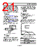
20 / 24 page  ADA4895-1/ADA4895-2 Data Sheet HIGH GAIN BANDWIDTH APPLICATION The circuit in Figure 52 shows cascaded dual amplifier stages using the ADA4895-1/ADA4895-2. Each stage has a gain of +10 (20 dB), making the output 100 times (40 dB) the input. The total gain bandwidth product is approximately 9 GHz with the device operating on 6 mA of quiescent current (3 mA per amplifier). VOUT VIN RT 50 Ω RL 1k Ω RF 226 Ω CF 2pF C1 5pF RG 25.5 Ω RF 226 Ω CF 2pF RG 25.5 Ω R1 249 Ω Figure 52. Cascaded Amplifier Stages for High Gain Applications (G = +100) Figure 53 shows the large signal frequency response for two cases. The first case is with installed feedback capacitors (CF = 2 pF), and the second case is without these capacitors. Removing the 2 pF feedback capacitors from this circuit increases the bandwidth, but adds about 0.5 dB of peaking. 0 4 8 12 16 20 24 28 32 36 40 44 0.1 1 10 100 1000 FREQUENCY (MHz) CF = 2pF NO CF VOUT = 2V p-p G = +100 Figure 53. Large Signal Frequency Response, G = +100, VS = ±5 V To better balance the second stage and remove the current offset contribution, an R1C1 circuit can be sized to correct for any mis-match between the source impedance and the feedback network impedance on the input amplifier. (In the example shown in Figure 52, R1 = 249 Ω and C1 = 5 pF.) The offset of each amplifier is within the same statistical range. As configured, the offset of the output amplifier is not statistically significant to the overall offset of the system. Figure 53 was captured using a ±5 V supply; however, this circuit also operates with supplies from ±1.5 V to ±5 V as long as the input and output headroom values are not violated. FEEDBACK CAPACITOR APPLICATION For applications where frequency response flatness is necessary, or a larger feedback resistor value is desired, a small feedback capacitor in parallel with the feedback resistor can be used to reduce peaking and increase flatness. Figure 54 shows the small signal frequency response with and without a feedback capacitor. –15 –12 –9 –6 –3 0 3 6 1 10 100 1000 FREQUENCY (MHz) RF = 449Ω RF = 1kΩ RF = 1kΩ, CF = 0.5pF RF = 499Ω, CF = 1pF VS = ±2.5V VOUT = 200mV p-p RL = 1kΩ G = +10 ADA4895-1 SOIC Figure 54. Small Signal Frequency Response With and Without a Feedback Capacitor Rev. B | Page 20 of 24 |
|
|
链接网址 |
| ALLDATASHEET是否为您带来帮助? [ DONATE ] |
关于 Alldatasheet | 广告服务 | 联系我们 | 隐私政策 | 数据表链接 | 链接交换 | 制造商名单 All Rights Reserved©Alldatasheet.com |
| Russian : Alldatasheetru.com | Korean : Alldatasheet.co.kr | Spanish : Alldatasheet.es | French : Alldatasheet.fr | Italian : Alldatasheetit.com Portuguese : Alldatasheetpt.com | Polish : Alldatasheet.pl | Vietnamese : Alldatasheet.vn Indian : Alldatasheet.in | Mexican : Alldatasheet.com.mx | British : Alldatasheet.co.uk | New Zealand : Alldatasheet.co.nz |
|
Family Site : ic2ic.com |
icmetro.com |
 Chinese ▼
 English
 Chinese
 German
 Japanese
 Russian
 Korean
 Spanish
 French
 Italian
 Portuguese
 Polish
 Vietnamese
 Indian
 Mexican
 British
 New Zealand