|
数据搜索系统,热门电子元器件搜索 |
|
|
数据搜索系统,热门电子元器件搜索 |
|
ADR510ART-R2 数据表(PDF) 5 Page - Analog Devices |
|
|
|||||||||||||||||||||||||||||
ADR510ART-R2 数据表(HTML) 5 Page - Analog Devices |
|
|
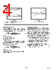
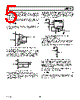
5 / 8 page  REV. 0 ADR510 –5– Adjustable Precision Voltage Source The ADR510, combined with a precision low input bias op amp such as the AD8610, can be used to output a precise adjustable voltage. Figure 2 illustrates the implementation of this application using the ADR510. The output of the op amp, VOUT, is determined by the gain of the circuit, which is completely dependent on Resistors R2 and R1. V R2 R1 OUT =+ 1 (4) An additional capacitor in parallel with R2 can be added to filter out high frequency noise. The value of C2 is dependent on the value of R2. VOUT = (1 + R2/R1) RBIAS R1 VCC R2 AD8610 ADR510 1.0V C2 (OPTIONAL) Figure 2. Adjustable Precision Voltage Source Output Voltage Trim Using a mechanical or digital potentiometer, the output voltage of the ADR510 can be trimmed ±0.5%. The circuit in Figure 3 illustrates how the output voltage can be trimmed, using a 10 k Ω potentiometer. Note that trimming using other resistor values may not produce an accurate output from the ADR510. RBIAS VCC R1 470k POT 10k ADR510 VOUT Figure 3. Output Voltage Trim Using the ADR510 with Precision Data Converters The compact ADR510 and its low minimum operating current requirement make it ideal for use in battery-powered portable instruments, such as the AD7533 CMOS multiplying DAC, that use precision data converters. Figure 4 shows the ADR510 serving as an external reference to the AD7533, a CMOS multiplying DAC. Such a DAC requires a negative voltage input in order to provide a positive output range. In this application, the ADR510 is supplying a –1.0 V reference to the REF input of the AD7533. MSB VDD VOUT = 0V TO 1.0V –VDD GN LSB 1 2 3 1 1 15 09 R2 ADR510 AD7533 Figure 4. ADR510 as a Reference for a 10-Bit CMOS DAC (AD7533) Precise Negative Voltage Reference The ADR510 is suitable for use in applications where a precise negative voltage reference is desired, including the application detailed in Figure 4. Figures 5 shows the ADR510 configured to provide a –1.0 V output. –1.0V –VDD R1 ADR510 Figure 5. Precise –1.0 V Reference Configuration Since the ADR510 characteristics resemble those of a Zener diode, the cathode shown in Figure 5 will be 1.0 V higher with respect to the anode (V+ with respect to V– on the ADR510 package). Since the cathode of the ADR510 is tied to ground, the anode must be –1.0 V. R1 in Figure 5 should be chosen so that 100 µA to 10 mA is provided to properly bias the ADR510. R V I DD 1 = (5) The R1 resistor should be chosen so that power dissipation is at a minimum. An ideal resistor value can be determined through manipulation of Equation 5. |
|
|
链接网址 |
| ALLDATASHEET是否为您带来帮助? [ DONATE ] |
关于 Alldatasheet | 广告服务 | 联系我们 | 隐私政策 | 数据表链接 | 链接交换 | 制造商名单 All Rights Reserved©Alldatasheet.com |
| Russian : Alldatasheetru.com | Korean : Alldatasheet.co.kr | Spanish : Alldatasheet.es | French : Alldatasheet.fr | Italian : Alldatasheetit.com Portuguese : Alldatasheetpt.com | Polish : Alldatasheet.pl | Vietnamese : Alldatasheet.vn Indian : Alldatasheet.in | Mexican : Alldatasheet.com.mx | British : Alldatasheet.co.uk | New Zealand : Alldatasheet.co.nz |
|
Family Site : ic2ic.com |
icmetro.com |
 Chinese ▼
 English
 Chinese
 German
 Japanese
 Russian
 Korean
 Spanish
 French
 Italian
 Portuguese
 Polish
 Vietnamese
 Indian
 Mexican
 British
 New Zealand