|
数据搜索系统,热门电子元器件搜索 |
|
|
数据搜索系统,热门电子元器件搜索 |
|
AD8652ARMZ-R2 数据表(PDF) 14 Page - Analog Devices |
|
|
|||||||||||||||||||||||||||||
AD8652ARMZ-R2 数据表(HTML) 14 Page - Analog Devices |
|
|
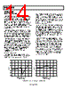
14 / 20 page  AD8651/AD8652 Rev. B | Page 14 of 20 APPLICATIONS THEORY OF OPERATION The AD8651 amplifier is a voltage feedback, rail-to-rail input and output precision CMOS amplifier that operates from 2.7 V to 5.0 V of power supply voltage. This amplifier uses Analog Devices’ DigiTrim technology to achieve a higher degree of precision than is available from most CMOS amplifiers. DigiTrim technology, used in a number of ADI amplifiers, is a method of trimming the offset voltage of the amplifier after it has been assembled. The advantage of post-package trimming is that it corrects any offset voltages caused by the mechanical stresses of assembly. The AD8651 is available in standard op amp pinout, making DigiTrim completely transparent to the user. The input stage of the amplifier is a true rail-to-rail architecture, allowing the input common-mode voltage range of the op amp to extend to both positive and negative supply rails. The open-loop gain of the AD8651/AD8652 with a load of 1 kΩ is typically 115 dB. The AD8651 can be used in any precision op amp application. The amplifier does not exhibit phase reversal for common- mode voltages within the power supply. With voltage noise of 4.5 nV/√Hz and –105 dB distortion for 10 kHz, 2 V p-p signals, the AD8651/AD8652 is a great choice for high resolution data acquisition systems. Its low noise, sub-pA input bias current, precision offset, and high speed make it a superb preamp for fast photodiode applications. The speed and output drive capability of the AD8651 also make it useful in video applications. Rail-to-Rail Output Stage The voltage swing of the output stage is rail-to-rail and is achieved by using an NMOS and PMOS transistor pair con- nected in a common source configuration. The maximum output voltage swing is proportional to the output current, and larger currents will limit how close the output voltage can get to the proximity of the output voltage to the supply rail. This is a characteristic of all rail-to-rail output amplifiers. With 40 mA of output current, the output voltage can reach within 5 mV of the positive and negative rails. At light loads of >100 kΩ, the output swings within ~1 mV of the supplies. Rail-to-Rail Input Stage The input common-mode voltage range of the AD8651 extends to both positive and negative supply voltages. This maximizes the usable voltage range of the amplifier, an important feature for single-supply and low voltage applications. This rail-to-rail input range is achieved by using two input differential pairs, one NMOS and one PMOS, placed in parallel. The NMOS pair is active at the upper end of the common-mode voltage range, and the PMOS pair is active at the lower end of the common- mode range. The NMOS and PMOS input stages are separately trimmed using DigiTrim to minimize the offset voltage in both differen- tial pairs. Both NMOS and PMOS input differential pairs are active in a 500 mV transition region when the input common- mode voltage is approximately 1.5 V below the positive supply voltage. A special design technique improves the input offset voltage in the transition region that traditionally exhibits a slight VOS variation. As a result, the common-mode rejection ratio is improved within this transition band. Compared to the Burr Brown OPA350 amplifier, shown in Figure 53 (A), the AD8651, shown in Figure 53 (B), exhibits much lower offset voltage shift across the entire input common-mode range, including the transition region. COMMON-MODE VOLTAGE (V) 0 –600 –200 200 600 400 0 –400 2 14 35 6 COMMON-MODE VOLTAGE (V) 0 –600 –200 200 600 400 0 –400 2 14 35 6 (A) OPA350 VOS vs. VCM (B) AD8651 VOS vs. VCM Figure 53. Input Offset Distribution over Common-Mode Voltage |
|
|
链接网址 |
| ALLDATASHEET是否为您带来帮助? [ DONATE ] |
关于 Alldatasheet | 广告服务 | 联系我们 | 隐私政策 | 数据表链接 | 链接交换 | 制造商名单 All Rights Reserved©Alldatasheet.com |
| Russian : Alldatasheetru.com | Korean : Alldatasheet.co.kr | Spanish : Alldatasheet.es | French : Alldatasheet.fr | Italian : Alldatasheetit.com Portuguese : Alldatasheetpt.com | Polish : Alldatasheet.pl | Vietnamese : Alldatasheet.vn Indian : Alldatasheet.in | Mexican : Alldatasheet.com.mx | British : Alldatasheet.co.uk | New Zealand : Alldatasheet.co.nz |
|
Family Site : ic2ic.com |
icmetro.com |
 Chinese ▼
 English
 Chinese
 German
 Japanese
 Russian
 Korean
 Spanish
 French
 Italian
 Portuguese
 Polish
 Vietnamese
 Indian
 Mexican
 British
 New Zealand