|
数据搜索系统,热门电子元器件搜索 |
|
|
数据搜索系统,热门电子元器件搜索 |
|
PLL702-06SCL-R 数据表(PDF) 4 Page - PhaseLink Corporation |
|
|
|||||||||||||||||||||||||||||
PLL702-06SCL-R 数据表(HTML) 4 Page - PhaseLink Corporation |
|
|
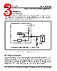
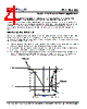
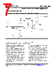
4 / 8 page  PLL702-06 Clock Generator for Printer Applications 47745 Fremont Blvd., Fremont, California 94538 Tel (510) 492-0990 Fax (510) 492-0991 www.phaselink.com Rev 10/26/05 Page 4 Note: when the output load presents a low impedance in comparison to the internal pull-up resistor, the internal pull-up resistor may not be sufficient to pull the input up to a logical “one”, and an external pull-up resistor may be required. For bi-directional inputs, the external loading resistor between the pin and GND has to be sufficiently small (compared to the internal pull-up resistor) so that the pin voltage be pulled below 0.8V (logical “zero”). In order to avoid loading effects when the pin serves as output, the value of the external pull-down resistor should however be kept as large as possible. In general, it is recommended to use an external resistor of around one sixth to one quarter of the internal pull-up resistor (see Application Diagram). VDD Power Up Ramp Requirements: At startup, the chip reads a lot of settings for operation according to the application’s requirements. Since reading the settings is done only at startup and then frozen for the time of operation, it is important that the power-up environment is somewhat controlled to facilitate proper reading of the settings. The important VDD pins are VDDA (Pin3) and VDDD (Pin4) and they should apply to the following two-startup requirements: • VDDD should be equally fast or slower than VDDA. VDDD performs a chip reset when VDD has reached a certain level and VDDA should have reached at least up to the same level as well to properly process the reset. • The VDD Power Up Ramp of VDDD and VDDA should pass through the section 1.8V to 2.5V no faster than 100µs and with a continuously increasing slope. In this section the tri-level select inputs are read. • After VDD Power off, VDD should be allowed to go to 0V and stay there for at least 1ms before a new VDD Power on. It is important that proper preconditions exist at every startup. Remaining charges in the chip or in circuit filter capacitors may interfere with the preconditions so it is important that VDD has been at 0V for some time before each startup. GND (0V) 3.3V No limit Min 1ms VDD off VDD on 2.97V 2.5V 2.2V Min 1s Reset enable Reset disable 1.8 V >100us |
|
|
链接网址 |
| ALLDATASHEET是否为您带来帮助? [ DONATE ] |
关于 Alldatasheet | 广告服务 | 联系我们 | 隐私政策 | 数据表链接 | 链接交换 | 制造商名单 All Rights Reserved©Alldatasheet.com |
| Russian : Alldatasheetru.com | Korean : Alldatasheet.co.kr | Spanish : Alldatasheet.es | French : Alldatasheet.fr | Italian : Alldatasheetit.com Portuguese : Alldatasheetpt.com | Polish : Alldatasheet.pl | Vietnamese : Alldatasheet.vn Indian : Alldatasheet.in | Mexican : Alldatasheet.com.mx | British : Alldatasheet.co.uk | New Zealand : Alldatasheet.co.nz |
|
Family Site : ic2ic.com |
icmetro.com |
 Chinese ▼
 English
 Chinese
 German
 Japanese
 Russian
 Korean
 Spanish
 French
 Italian
 Portuguese
 Polish
 Vietnamese
 Indian
 Mexican
 British
 New Zealand