|
数据搜索系统,热门电子元器件搜索 |
|
|
数据搜索系统,热门电子元器件搜索 |
|
AM6441...ALV 数据表(PDF) 8 Page - Texas Instruments |
|
|
|||||||||||||||||||||||||||||
AM6441...ALV 数据表(HTML) 8 Page - Texas Instruments |
|
|
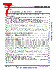
8 / 244 page  • (Absolute Maximum Ratings): Added USB0_ID and associated note to define its absolute maximum ratings.... ..........................................................................................................................................................................98 • (Absolute Maximum Ratings): Added VMON_VSYS to the paragraph that is describing Fail-safe IO terminals ..........................................................................................................................................................................98 • (Recommended Operating Conditions): Added USB0_ID and associated note to define its recommended operating conditions........................................................................................................................................101 • (I2C OD FS Electrical Characteristics): Added a note to explain the IOL parameter.......................................102 • (SDIO Electrical Characteristics): Added a note to explain the IOL and IOH parameters.................................104 • (LVCMOS Electrical Characteristics): Added a note to explain the IOL and IOH parameters.......................... 105 • (Recommended Operating Conditions for OTP eFuse Programming): Changed the maximum VPP current value from TBD to 400 mA............................................................................................................................. 109 • (Power Supply Requirements): Updated the section title from "Power Supply Sequencing" to "Power Supply Requirements"................................................................................................................................................ 112 • (Power Supply Sequencing): Added new section and explaination of the two types of power supply transition regions found in the Power-up and Power-down Sequence diagrams........................................................... 113 • (MCU_OSC0 Start-up Time): Updated signal names in figure....................................................................... 124 • (GPMC and NOR Flash — Synchronous Mode): Updated timing parameters and values............................ 143 • (GPMC and NOR Flash — Asynchronous Mode): Updated timing parameters and values...........................152 • (GPMC and NAND Flash — Asynchronous Mode): Updated timing parameters and values........................ 160 • (MMCSD): Added a new paragraph to the note that explains the meaning of "Tuning" in the MMC0 DLL Delay Mapping and MMC1 DLL Delay Mapping tables ........................................................................................... 172 • (MMC0 DLL Delay Mapping for All Timing Modes): Added notes to describe the meaning of "NA" and "Tuning".......................................................................................................................................................... 173 • (MMC1 DLL Delay Mapping for All Timing Modes): Added a note to describe the meaning of "Tuning"....... 177 • (Switching Characteristics for MMC1 – UHS-I SDR12 Mode): Changed "falling" to "rising" in the description of timing paramter SDR128 and SDR129...........................................................................................................181 • (Switching Characteristics for MMC1 – UHS-I SDR25 Mode): Changed "falling" to "rising" in the description of timing paramter SDR258 and SDR259...........................................................................................................182 • (OSPI): Updated the entire OSPI timing section.............................................................................................186 • (PRU_ICSSG): Updated the note to use the same description used in the PRU_ICSSG Signal Description note.................................................................................................................................................................194 • (PRU_ICSSG PRU Parallel Capture Mode Timing): Updated minimum pulse duration values for CLOCKIN, parameters PRPC2 and PRPC3.....................................................................................................................195 • (PRU_ICSSG PRU Switching Characteristics - Shift Out Mode): Corrected errors in notes associated with variables Z and Y............................................................................................................................................196 • (PRU_ICSSG IEP Timing Conditions): Updated output load capacitance to include a different minimum to maximum range for EDIO_DATA_OUT.......................................................................................................... 200 • (PRU_ICSSG IEP Timing): Changed the title of the "PRU_ICSSG IEP Timing Requirements – Digital IOs" table to "PRU_ICSSG IEP Switching Characteristics – Digital IOs" and changed the values defined for parameter IEPO4............................................................................................................................................200 • (PRU_ICSSG UART Timing): Updated timing parameter values................................................................... 201 • (PRU_ICSSG ECAP Switching Characteristics): Updated the minimum pulse duration values, parameters PREP3 and PREP4........................................................................................................................................ 202 • (PRU_ICSSG RGMII Timing Conditions): Updated Input Slew Rate and added PCB Connectivity Requirements................................................................................................................................................. 206 • (JTAG Timing Conditions): Added PCB Connectivity Requirements to the Timing Conditions table..............211 • (JTAG Timing Requirements): Added a note to the minimum TCK cycle time parameter.............................. 211 • (I2C module features): Updated FIFO size, and clarified high-speed mode is only supported on I2C0 and MCU_I2C0...................................................................................................................................................... 219 • (No Loopback, Internal Pad Loopback, and Internal Pad Loopback): Section title was changed to include "Internal Pad Loopback", updated the decriptions for propagation delay and trace length matching requirements, removed the "MCU_" prefix from signal names, changed the title of the OSPI connectivity schematic, and updated the OSPI connectivity schematic to include all of the OSPI pins.............................227 AM6442, AM6441, AM6421, AM6412, AM6411 SPRSP56D – JANUARY 2021 – REVISED JULY 2022 www.ti.com 8 Submit Document Feedback Copyright © 2022 Texas Instruments Incorporated Product Folder Links: AM6442 AM6441 AM6421 AM6412 AM6411 |
|
链接网址 |
| ALLDATASHEET是否为您带来帮助? [ DONATE ] |
关于 Alldatasheet | 广告服务 | 联系我们 | 隐私政策 | 数据表链接 | 链接交换 | 制造商名单 All Rights Reserved©Alldatasheet.com |
| Russian : Alldatasheetru.com | Korean : Alldatasheet.co.kr | Spanish : Alldatasheet.es | French : Alldatasheet.fr | Italian : Alldatasheetit.com Portuguese : Alldatasheetpt.com | Polish : Alldatasheet.pl | Vietnamese : Alldatasheet.vn Indian : Alldatasheet.in | Mexican : Alldatasheet.com.mx | British : Alldatasheet.co.uk | New Zealand : Alldatasheet.co.nz |
|
Family Site : ic2ic.com |
icmetro.com |
 Chinese ▼
 English
 Chinese
 German
 Japanese
 Russian
 Korean
 Spanish
 French
 Italian
 Portuguese
 Polish
 Vietnamese
 Indian
 Mexican
 British
 New Zealand