|
数据搜索系统,热门电子元器件搜索 |
|
|
数据搜索系统,热门电子元器件搜索 |
|
P9221-R 数据表(PDF) 8 Page - Renesas Technology Corp |
|
|
|||||||||||||||||||||||||||||
P9221-R 数据表(HTML) 8 Page - Renesas Technology Corp |
|
|
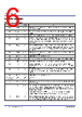
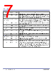
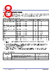
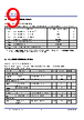
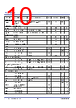
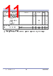
8 / 38 page  P9221-R Datasheet © 2017 Integrated Device Technology, Inc. 8 October 10, 2017 3. Absolute Maximum Ratings Stresses greater than those listed as absolute maximum ratings in Table 2 could cause permanent damage to the device. These are stress ratings only, and functional operation of the device at these or any other conditions above those indicated in the operational sections of this specification is not implied. Exposure to absolute maximum rating conditions for extended periods might affect reliability. Table 2. Absolute Maximum Ratings Pins[a],[b] Parameter Conditions Minimum[c] Maximum[c] Units AC1[d], AC2[d], COMM1, COMM2 Absolute Maximum Pin Voltage -0.3 20 V EN ̅̅̅̅ Absolute Maximum Pin Voltage -0.3 28 V SINK, VRECT Absolute Maximum Pin Voltage -0.3 24 V DEN, ILIM, RPPG, RPPO, VDD18, VOSET Absolute Maximum Pin Voltage -0.3 2 V ALIGNX, ALIGNY, INT ̅̅̅̅, SCL, SDA, TS, VDD5V Absolute Maximum Pin Voltage -0.3 6 V BST1 Absolute Maximum Pin Voltage -0.3 AC1 + 6 V BST2 Absolute Maximum Pin Voltage -0.3 AC2 + 6 V OUT Absolute Maximum Pin Voltage -0.3 14.4 V SINK Maximum Current on Pin – 1 A COMM1, COMM2 Maximum RMS Current on Pin – 500 mA AC1, AC2 Maximum RMS Current from Pin – 2 A [a] Absolute maximum ratings are not provided for reserved pins (RSV1, RSV2, RSV3, RSV4, RSV5, and DEN). These pins are not used in the application. [b] For the test conditions for the absolute maximum ratings specifications, the P9221-R characterization for the operating ambient temperature (TAMB) specification (see Table 4) has been performed down to -10°C only. Design simulation indicates normal operation down to -45°C. Limited bench functionality tests indicate normal operation down to -40°C. [c] All voltages are referred to ground unless otherwise noted. [d] During synchronous rectifier dead time, the voltage on the AC1 and AC2 pins is developed by current across the internal power FET’s body diodes, and it might be lower than -0.3 V. This is a normal behavior and does not negatively impact the functionality or reliability of the product. Table 3. ESD Information Test Model Pins Ratings Units HBM All pins except RSV1, RSV2, RSV3, RSV4, and RSV5 pins 2 kV RSV1, RSV2, RSV3, RSV4, and RSV5 pins 1 kV CDM All pins 500 V |
|
链接网址 |
| ALLDATASHEET是否为您带来帮助? [ DONATE ] |
关于 Alldatasheet | 广告服务 | 联系我们 | 隐私政策 | 数据表链接 | 链接交换 | 制造商名单 All Rights Reserved©Alldatasheet.com |
| Russian : Alldatasheetru.com | Korean : Alldatasheet.co.kr | Spanish : Alldatasheet.es | French : Alldatasheet.fr | Italian : Alldatasheetit.com Portuguese : Alldatasheetpt.com | Polish : Alldatasheet.pl | Vietnamese : Alldatasheet.vn Indian : Alldatasheet.in | Mexican : Alldatasheet.com.mx | British : Alldatasheet.co.uk | New Zealand : Alldatasheet.co.nz |
|
Family Site : ic2ic.com |
icmetro.com |
 Chinese ▼
 English
 Chinese
 German
 Japanese
 Russian
 Korean
 Spanish
 French
 Italian
 Portuguese
 Polish
 Vietnamese
 Indian
 Mexican
 British
 New Zealand