|
数据搜索系统,热门电子元器件搜索 |
|
|
数据搜索系统,热门电子元器件搜索 |
|
P9221-R 数据表(PDF) 25 Page - Renesas Technology Corp |
|
|
|||||||||||||||||||||||||||||
P9221-R 数据表(HTML) 25 Page - Renesas Technology Corp |
|
|
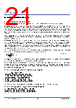
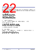
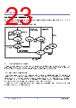
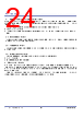
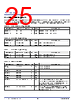
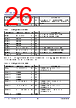
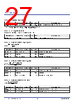
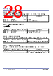
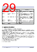
25 / 38 page  P9221-R Datasheet © 2017 Integrated Device Technology, Inc. 25 October 10, 2017 11. Functional Registers The following tables provide the address locations, field names, available operations (R or RW), default values, and functional descriptions of all the internally accessible registers contained within the P9221-R. The default I2 C slave address is 61HEX. The address of each register has a two-byte structure. For example, the low byte of major firmware revision must be read with two bytes address with 00HEX and 04HEX. Table 9. Device Identification Register Address and Bit Register or Bit Field Name R/W Default Function and Description 0000HEX [7:0] Part_number_L R 20HEX P9221-R chip identification low byte 0001HEX [7:0] Part_number_H R 92HEX P9221-R chip identification high byte Table 10. Firmware Major Revision Address and Bit Register or Bit Field Name R/W Default Function and Description 0004HEX [7:0] FW_Major_Rev_L R 01HEX Major firmware revision low byte 0005HEX [7:0] FW_Major_Rev_H R 00HEX Major firmware revision high byte Table 11. Firmware Minor Revision Address and Bit Register or Bit Field Name R/W Default Function and Description 0006HEX [7:0] FW_Minor_Rev_L R 29HEX Minor firmware revision low byte 0007HEX [7:0] FW_Minor_Rev_H R 04HEX Minor firmware revision high byte Table 12. Status Registers Address and Bit Register or Bit Field Name R/W Default Function and Description 0034HEX [7] Vout_Status R 0BIN “0” output voltage is off. “1” output voltage is on. 0034HEX [6] Reserved R 0BIN 0034HEX [5] Reserved R 0BIN 0034HEX [4] Reserved R 0BIN 0034HEX [3] Reserved R 0BIN 0034HEX [2] Thermal_SHTDN_Status R 0BIN “0” indicates no over-temperature condition exists. “1” indicates that the die temperature exceeds 130°C or the NTC reading is less than 0.6V. The P9221-R sends an End Power Transfer (EPT) packet to the transmitter. 0034HEX [1] VRECT_OV_Status R 0BIN “1” indicates the rectifier voltage exceeds 20V for VOUT=12V. In this case, the P9221-R sends an End Power Transfer (EPT) packet to the transmitter. |
|
链接网址 |
| ALLDATASHEET是否为您带来帮助? [ DONATE ] |
关于 Alldatasheet | 广告服务 | 联系我们 | 隐私政策 | 数据表链接 | 链接交换 | 制造商名单 All Rights Reserved©Alldatasheet.com |
| Russian : Alldatasheetru.com | Korean : Alldatasheet.co.kr | Spanish : Alldatasheet.es | French : Alldatasheet.fr | Italian : Alldatasheetit.com Portuguese : Alldatasheetpt.com | Polish : Alldatasheet.pl | Vietnamese : Alldatasheet.vn Indian : Alldatasheet.in | Mexican : Alldatasheet.com.mx | British : Alldatasheet.co.uk | New Zealand : Alldatasheet.co.nz |
|
Family Site : ic2ic.com |
icmetro.com |
 Chinese ▼
 English
 Chinese
 German
 Japanese
 Russian
 Korean
 Spanish
 French
 Italian
 Portuguese
 Polish
 Vietnamese
 Indian
 Mexican
 British
 New Zealand