SC-604
Data sheet
6
P/N 80-0208-B
© 2002 Sensory Inc.
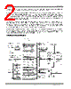
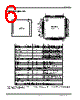
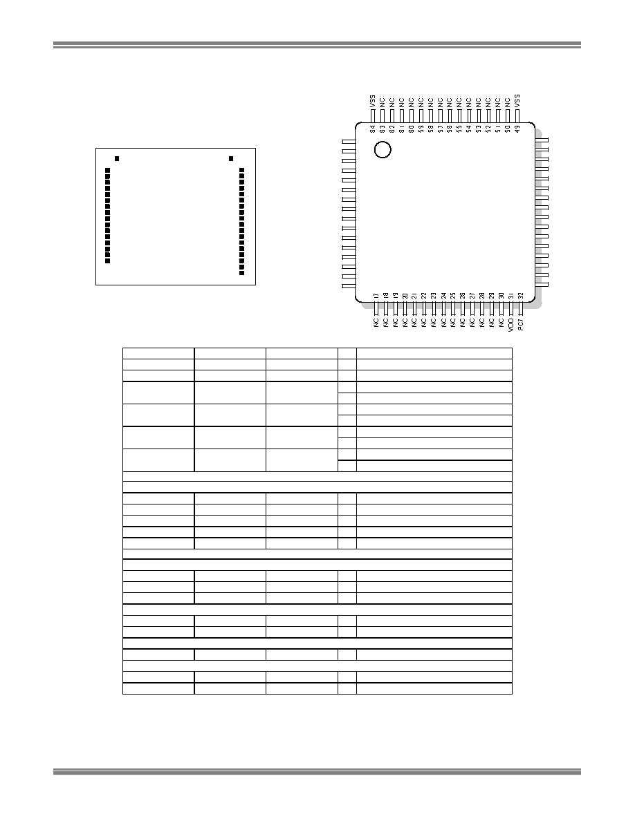
Pin/Pad Assignments
SC-604
(top view of the die)
36
1
16
35
17
34
SC-604
(64-lead LQFP)
VSS
DACP
PD5
PD6
PD7
PC0
PC1
48
47
42
41
40
39
38
PC2
PC3
PC4
37
36
35
VDD
46
DACM
VDD
PD4
45
44
43
PC5
34
PC6
33
VDD
VDD
R/W_
STROBE_
OUTRDY_
INRDY_
TEST
SCANOUT
SYNC
SCANCLK
SCANIN
RESET_
1
2
3
4
5
6
7
8
9
10
11
12
PLL
OSCIN
OSCOUT
VSS
13
14
15
16
NAME
PIN NO.
PAD NO.
I/O DESCRIPTION
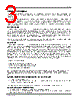
PC0 – PC7
39 → 32
25 → 18
I/O Port C general-purpose I/O (1 Byte)
PD4 – PD7
43 → 40
29 → 26
I/O Port D general-purpose I/O (1 Byte)
I/O (Master) Port D general-purpose I/O
PD0/INRDY
6
6
O (Slave) INRDY output to host
I/O (Master) Port D general-purpose I/O
PD1/OUTRDY_
5
5
O (Slave) OUTRDY_ output to host
I/O (Master) Port D general-purpose I/O
PD2/STROBE_
4
4
O (Slave) STROBE_ input from host
I/O (Master) Port D general-purpose I/O
PD3/R/W_
3
3
O (Slave) Read/write input from host
Pins PD4 and PD5 may be dedicated to the comparator function, if the comparator enable bit is set.
Scan Port Control Signals
SCANIN
11
11
I
Scan port data input
SCANOUT
8
8
O Scan port data output
SCANCLK
10
10
I
Scan port clock
SYNC
9
9
I
Scan port synchronization
TEST
7
7
I
Test modes
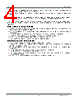
The scan port pins must be bonded out on any SC-604 production board.
Reference Oscillator Signals
OSCOUT
15
15
O Resistor/crystal reference out
OSCIN
14
14
I
Resistor/crystal reference in
PLL
13
13
O Phase-lock-loop filter
Digital-to-Analog Sound Output
DACP
47
33
O Digital-to-analog plus output (+)
DACM
45
31
O Digital-to-analog minus output (–)
Initialization
RESET_
12
12
I
Initialization
Power Signals
VSS
16, 48, 49
†, 64 16, 34†, 35, 36
-
Ground
VDD
1, 2, 31, 44, 46
† 1, 2, 17, 30, 32† - Processor power (+)
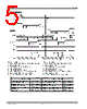
† The VSS and VDD connections service the DAC circuitry. Their pins tend to sustain a higher current draw. A dedicated decoupling capacitor
across these pins is therefore required.

 Chinese ▼
 English
 Chinese
 German
 Japanese
 Russian
 Korean
 Spanish
 French
 Italian
 Portuguese
 Polish
 Vietnamese
 Indian
 Mexican
 British
 New Zealand