|
数据搜索系统,热门电子元器件搜索 |
|
|
数据搜索系统,热门电子元器件搜索 |
|
ADCMP603BCPZ-R7 数据表(PDF) 12 Page - Analog Devices |
|
|
|||||||||||||||||||||||||||||
ADCMP603BCPZ-R7 数据表(HTML) 12 Page - Analog Devices |
|
|
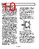
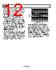
12 / 16 page  ADCMP603 Rev. 0 | Page 12 of 16 50 150 250 350 450 550 650 HYSTERESIS RESISTOR (kΩ) 1 10 100 1000 VCC = 5.5V VCC = 2.5V The ADCMP603 comparator offers a programmable hysteresis feature that can significantly improve accuracy and stability. Connecting an external pull-down resistor or a current source from the LE/HYS pin to GND varies the amount of hysteresis in a predictable, stable manner. Leaving the LE/HYS pin disconnected or driving it high removes the hysteresis. The maximum hysteresis that can be applied using this pin is approximately 160 mV. Figure 18 illustrates the amount of hysteresis applied as a function of the external resistor value, and Figure 9 illustrates hysteresis as a function of the current. The hysteresis control pin appears as a 1.25 V bias voltage seen through a series resistance of 7 kΩ ± 20% throughout the hysteresis control range. The advantages of applying hysteresis in this manner are improved accuracy, improved stability, reduced component count, and maximum versatility. An external bypass capacitor is not recommended on the HYS pin because it impairs the latch function and often degrades the jitter performance of the device. As described in the Using/Disabling the Latch Feature section, hysteresis control need not compromise the latch function. Figure 18. Hysteresis vs. R Control Resistor HYS MINIMUM INPUT SLEW RATE REQUIREMENT With the rated load capacitance and normal good PC Board design practice, as discussed in the Optimizing Performance section, these comparators should be stable at any input slew rate with no hysteresis. Broadband noise from the input stage is observed in place of the violent chattering seen with most other high speed comparators. With additional capacitive loading or poor bypassing, more persistent oscillations are seen. This oscillation is due to the high gain bandwidth of the comparator in combination with feedback parasitics in the package and PC board. In many applications, chattering is not harmful since the first cycle of the oscillation occurs close to V CROSSOVER BIAS POINT In both op amps and comparators, rail-to-rail inputs of this type have a dual front-end design. Certain devices are active near the VCC rail and others are active near the VEE rail. At some predeter- mined point in the common-mode range, a crossover occurs. At this point, typically VCC/2, the direction of the bias current reverses and the measured offset voltages and currents change. OS . The ADCMP603 slightly elaborates on this scheme. Crossover points can be found at approximately 0.8 V and 1.6 V. |
|
|
链接网址 |
| ALLDATASHEET是否为您带来帮助? [ DONATE ] |
关于 Alldatasheet | 广告服务 | 联系我们 | 隐私政策 | 数据表链接 | 链接交换 | 制造商名单 All Rights Reserved©Alldatasheet.com |
| Russian : Alldatasheetru.com | Korean : Alldatasheet.co.kr | Spanish : Alldatasheet.es | French : Alldatasheet.fr | Italian : Alldatasheetit.com Portuguese : Alldatasheetpt.com | Polish : Alldatasheet.pl | Vietnamese : Alldatasheet.vn Indian : Alldatasheet.in | Mexican : Alldatasheet.com.mx | British : Alldatasheet.co.uk | New Zealand : Alldatasheet.co.nz |
|
Family Site : ic2ic.com |
icmetro.com |
 Chinese ▼
 English
 Chinese
 German
 Japanese
 Russian
 Korean
 Spanish
 French
 Italian
 Portuguese
 Polish
 Vietnamese
 Indian
 Mexican
 British
 New Zealand