|
数据搜索系统,热门电子元器件搜索 |
|
|
数据搜索系统,热门电子元器件搜索 |
|
AD8571ARMZ-R2 数据表(PDF) 14 Page - Analog Devices |
|
|
|||||||||||||||||||||||||||||
AD8571ARMZ-R2 数据表(HTML) 14 Page - Analog Devices |
|
|
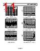
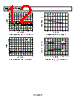
14 / 24 page  AD8571/AD8572/AD8574 Rev. B | Page 14 of 24 FUNCTIONAL DESCRIPTION The AD8571/AD8572/AD8574 are CMOS amplifiers that achieve their high degree of precision through random frequency auto-zero stabilization. The autocorrection topology allows the AD857x to maintain its low offset voltage over a wide temperature range, and the randomized auto-zero clock eliminates any intermodulation distortion (IMD) errors at the amplifier output. The AD857x can be run from a single-supply voltage as low as 2.7 V. The extremely low offset voltage of 1 μV and no IMD products allows the amplifier to be easily configured for high gains without risk of excessive output voltage errors. This makes the AD857x an ideal amplifier for applications requiring both dc precision and low distortion for ac signals. The extremely small temperature drift of 5 nV/°C ensures a minimum of offset voltage error over its entire temperature range of −40°C to +125°C. These combined features make the AD857x an excellent choice for a variety of sensitive measurement and automotive applications. AMPLIFIER ARCHITECTURE Each AD857x op amp consists of two amplifiers: a main amplifier and a secondary amplifier that is used to correct the offset voltage of the main amplifier. Both consist of a rail-to-rail input stage, allowing the input common-mode voltage range to reach both supply rails. The input stage consists of an NMOS differential pair operating concurrently with a parallel PMOS differential pair. The outputs from the differential input stages are combined in another gain stage whose output is used to drive a rail-to-rail output stage. The wide voltage swing of the amplifier is achieved by using two output transistors in a common-source configuration. The output voltage range is limited by the drain-to-source resistance of these transistors. As the amplifier is required to source or sink more output current, the voltage drop across these transistors increases due to their on resistance (rds). Simply put, the output voltage does not swing as close to the rail under heavy output current conditions as it does with light output current. This is a characteristic of all rail-to-rail output amplifiers. Figure 12 and Figure 13 show how close the output voltage can get to the rails with a given output current. The output of the AD857x is short- circuit protected to approximately 50 mA of current. The AD857x amplifiers have exceptional gain, yielding greater than 120 dB of open-loop gain with a load of 2 kΩ. Because the output transistors are configured in a common-source configura- tion, the gain of the output stage, and thus the open-loop gain of the amplifier, is dependent on the load resistance. Open-loop gain decreases with smaller load resistances. This is another characteristic of rail-to-rail output amplifiers. BASIC AUTO-ZERO AMPLIFIER THEORY Autocorrection amplifiers are not a new technology. Various IC implementations have been available for more than 15 years and some improvements have been made over time. The AD857x design offers a number of significant performance improve- ments over older versions while attaining a very substantial reduction in device cost. This section offers a simplified explanation of how the AD857x is able to offer extremely low offset voltages and high open-loop gains. As noted in the Amplifier Architecture section, each AD857x op amp contains two internal amplifiers. One is used as the primary amplifier, the other as an autocorrection, or nulling, amplifier. Each amplifier has an associated input offset voltage that can be modeled as a dc voltage source in series with the noninverting input. In Figure 50 and Figure 51, these are labeled as VOSX, where X denotes the amplifier associated with the offset: A for the nulling amplifier, B for the primary amplifier. The open-loop gain for the +IN and −IN inputs of each amplifier is given as AX. Both amplifiers also have a third voltage input with an associated open-loop gain of BX. There are two modes of operation determined by the action of two sets of switches in the amplifier: an auto-zero phase and an amplification phase. AUTO-ZERO PHASE In this phase, all φA switches are closed and all φB switches are opened. Here, the nulling amplifier is taken out of the gain loop by shorting its two inputs together. Of course, there is a degree of offset voltage, shown as VOSA, inherent in the nulling amplifier that maintains a potential difference between the +IN and −IN inputs. The nulling amplifier feedback loop is closed through φA2 and VOSA appears at the output of the nulling amp and on CM1, an internal capacitor in the AD857x. Mathematically, we can express this in the time domain as ] [ ] [ ] [ t V B t V A t V OA A OSA A OA − = (1) this also can be expressed as [] [ ] A OSA A OA B t V A t V + = 1 (2) This shows that the offset voltage of the nulling amplifier times a gain factor appears at the output of the nulling amplifier and thus on the CM1 capacitor. |
|
|
链接网址 |
| ALLDATASHEET是否为您带来帮助? [ DONATE ] |
关于 Alldatasheet | 广告服务 | 联系我们 | 隐私政策 | 数据表链接 | 链接交换 | 制造商名单 All Rights Reserved©Alldatasheet.com |
| Russian : Alldatasheetru.com | Korean : Alldatasheet.co.kr | Spanish : Alldatasheet.es | French : Alldatasheet.fr | Italian : Alldatasheetit.com Portuguese : Alldatasheetpt.com | Polish : Alldatasheet.pl | Vietnamese : Alldatasheet.vn Indian : Alldatasheet.in | Mexican : Alldatasheet.com.mx | British : Alldatasheet.co.uk | New Zealand : Alldatasheet.co.nz |
|
Family Site : ic2ic.com |
icmetro.com |
 Chinese ▼
 English
 Chinese
 German
 Japanese
 Russian
 Korean
 Spanish
 French
 Italian
 Portuguese
 Polish
 Vietnamese
 Indian
 Mexican
 British
 New Zealand