|
数据搜索系统,热门电子元器件搜索 |
|
|
数据搜索系统,热门电子元器件搜索 |
|
AD8571ARMZ-R2 数据表(PDF) 21 Page - Analog Devices |
|
|
|||||||||||||||||||||||||||||
AD8571ARMZ-R2 数据表(HTML) 21 Page - Analog Devices |
|
|
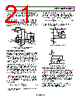
21 / 24 page  AD8571/AD8572/AD8574 Rev. B | Page 21 of 24 the thermocouple and should be placed as close as possible to the two terminating junctions. With the thermocouple measuring tip immersed in a 0°C ice bath, R6 should be adjusted until the output is at 0 V. Using the values shown in Figure 66, the output voltage tracks temperature at 10 mV/°C. For a wider range of temperature measurement, R9 can be decreased to 62 kΩ. This creates a 5 mV/°C change at the output, allowing measurements of up to 1000°C. AD8572 3 8 4 0V TO 5V (0°C TO 500°C) 5V 0.1µF 10µF REF02EZ 0.1µF 12V 2 6 4 ++ –– D1 1N4148 5V K-TYPE THERMOCOUPLE 40.7µV/°C 1 2 R2 2.74kΩ R6 200Ω R3 53.6kΩ R4 5.62kΩ R1 10.7kΩ R5 40.2kΩ R9 124kΩ R8 453Ω Figure 66. Precision K-Type Thermocouple Amplifier with Cold-Junction Compensation PRECISION CURRENT METER Because of its low input bias current and superb offset voltage at single-supply voltages, the AD857x is an excellent amplifier for precision current monitoring. Its rail-to-rail input allows the amplifier to be used as either a high-side or a low-side current monitor. Using both amplifiers in the AD8572 provides a simple method to monitor both current supply and return paths for load or fault detection. Figure 67 shows a high-side current monitor configuration. Here, the input common-mode voltage of the amplifier is at or near the positive supply voltage. The rail-to-rail input of the amplifier provides a precise measurement, even with the input common-mode voltage at the supply voltage. The CMOS input structure does not draw any input bias current, ensuring a minimum of measurement error. The 0.1 Ω resistor creates a voltage drop to the noninverting input of the AD857x. The output of the amplifier is corrected until this voltage appears at the inverting input. This creates a current through R1 that in turn flows through R2. The monitor output is given by L SENSE I 1 R R 2 R Output Monitor × ⎟ ⎠ ⎞ ⎜ ⎝ ⎛ × = (23) Using the components shown in Figure 67, the monitor output transfer function is 2.5 V/A. Figure 68 shows the low-side monitor equivalent. In this circuit, the input common-mode voltage to the AD8572 is at or near ground. Again, a 0.1 Ω resistor provides a voltage drop propor- tional to the return current. The output voltage is given as ⎟ ⎠ ⎞ ⎜ ⎝ ⎛ × × − + = L SENSE OUT I R 1 R 2 R V V (24) For the component values shown in Figure 68, the output transfer function decreases from V at –2.5 V/A. 8 1 4 3 3V 0.1µF V+ IL G S D 2 M1 Si9433 MONITOR OUTPUT 3V 1/2 AD8572 R1 100Ω R2 2.49kΩ RSENSE 0.1Ω Figure 67. High-Side Load Current Monitor V+ RETURN TO GROUND 1/2 AD8572 V+ VOUT Q1 RSENSE 0.1Ω R1 100Ω R2 2.49kΩ Figure 68. Low-Side Load Current Monitor PRECISION VOLTAGE COMPARATOR The AD857x can be operated open-loop and used as a precision comparator. The AD857x has less than 50 μV of offset voltage when run in this configuration. The slight increase of offset voltage stems from the fact that the autocorrection architecture operates with lowest offset in a closed-loop configuration, that is, one with negative feedback. With 50 mV of overdrive, the device has a propagation delay of 15 μs on the rising edge and 8 μs on the falling edge. Care should be taken to ensure the maximum differential voltage of the device is not exceeded. For more information, refer to the Input Overvoltage Protection section. |
|
|
链接网址 |
| ALLDATASHEET是否为您带来帮助? [ DONATE ] |
关于 Alldatasheet | 广告服务 | 联系我们 | 隐私政策 | 数据表链接 | 链接交换 | 制造商名单 All Rights Reserved©Alldatasheet.com |
| Russian : Alldatasheetru.com | Korean : Alldatasheet.co.kr | Spanish : Alldatasheet.es | French : Alldatasheet.fr | Italian : Alldatasheetit.com Portuguese : Alldatasheetpt.com | Polish : Alldatasheet.pl | Vietnamese : Alldatasheet.vn Indian : Alldatasheet.in | Mexican : Alldatasheet.com.mx | British : Alldatasheet.co.uk | New Zealand : Alldatasheet.co.nz |
|
Family Site : ic2ic.com |
icmetro.com |
 Chinese ▼
 English
 Chinese
 German
 Japanese
 Russian
 Korean
 Spanish
 French
 Italian
 Portuguese
 Polish
 Vietnamese
 Indian
 Mexican
 British
 New Zealand