|
数据搜索系统,热门电子元器件搜索 |
|
|
数据搜索系统,热门电子元器件搜索 |
|
ADL5330ACPZ-R2 数据表(PDF) 20 Page - Analog Devices |
|
|
|||||||||||||||||||||||||||||
ADL5330ACPZ-R2 数据表(HTML) 20 Page - Analog Devices |
|
|
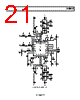
20 / 24 page  ADL5330 Rev. A | Page 20 of 24 EVALUATION BOARD Figure 49 shows the schematic of the ADL5330 evaluation board. The silkscreen and layout of the component and circuit sides are shown in Figure 50 through Figure 53. The board is powered by a single-supply in the 4.75 V to 5.25 V range. The power supply is decoupled by 100 pF and 0.1 μF capacitors at each power supply pin. Additional decoupling, in the form of a series resistor or inductor at the supply pins, can also be added. Table 5 details the various configuration options of the evaluation board. The output pins of the ADL5330 require supply biasing with 120 nH RF chokes. Both the input and output pins have 50 Ω differential impedances and must be ac-coupled. These pins are converted to single-ended with a pair of baluns (M/A-COM part number ETC1-1-13). Instead of using balun transformers, lumped-element baluns comprising passive L and C components can be designed. Alternate input and output RF paths with component pads are available on the circuit side of the board. Components M1 through M9 are used for the input interface, and M10 through M18 are used for the output interface. DC blocking capacitors of 100 pF must be installed in C15 and C16 for the input and C17 and C18 for the output. The C5, C6, C11, and C12 capacitors must be removed. An alternate set of SMA connectors, INPUT2 and OUT2, are used for this configuration. The ADL5330 can be driven single-ended; use the RF input path on the circuit side of the board. A set of 100 pF dc blocking capacitors must be installed in C15 and C16. C5 and C6 must be removed. Use the INPUT2 SMA to drive one of the differential input pins. The unused pin should be terminated to ground, as shown in Figure 34. The ADL5330 is enabled by applying a logic high voltage to the ENBL pin by placing a jumper across the SW1 header in the O position. Remove the jumper for disable. This pulls the ENBL pin to ground through the 10 kΩ resistor. |
|
|
链接网址 |
| ALLDATASHEET是否为您带来帮助? [ DONATE ] |
关于 Alldatasheet | 广告服务 | 联系我们 | 隐私政策 | 数据表链接 | 链接交换 | 制造商名单 All Rights Reserved©Alldatasheet.com |
| Russian : Alldatasheetru.com | Korean : Alldatasheet.co.kr | Spanish : Alldatasheet.es | French : Alldatasheet.fr | Italian : Alldatasheetit.com Portuguese : Alldatasheetpt.com | Polish : Alldatasheet.pl | Vietnamese : Alldatasheet.vn Indian : Alldatasheet.in | Mexican : Alldatasheet.com.mx | British : Alldatasheet.co.uk | New Zealand : Alldatasheet.co.nz |
|
Family Site : ic2ic.com |
icmetro.com |
 Chinese ▼
 English
 Chinese
 German
 Japanese
 Russian
 Korean
 Spanish
 French
 Italian
 Portuguese
 Polish
 Vietnamese
 Indian
 Mexican
 British
 New Zealand