|
数据搜索系统,热门电子元器件搜索 |
|
|
数据搜索系统,热门电子元器件搜索 |
|
AD8062ARMZ-R7 数据表(PDF) 14 Page - Analog Devices |
|
|
|||||||||||||||||||||||||||||
AD8062ARMZ-R7 数据表(HTML) 14 Page - Analog Devices |
|
|
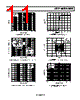
14 / 20 page  AD8061/AD8062/AD8063 Rev. D | Page 14 of 20 CIRCUIT DESCRIPTION The AD8061/AD8062/AD8063 family is comprised of high speed voltage feedback op amps. The high slew rate input stage is a true, single-supply topology, capable of sensing signals at or below the minus supply rail. The rail-to-rail output stage can pull within 30 mV of either supply rail when driving light loads and within 0.3 V when driving 150 Ω. High speed perform- ance is maintained at supply voltages as low as 2.7 V. HEADROOM CONSIDERATIONS These amplifiers are designed for use in low voltage systems. To obtain optimum performance, it is useful to understand the behavior of the amplifier as input and output signals approach the amplifier’s headroom limits. The AD806x’s input common-mode voltage range extends from the negative supply voltage (actually 200 mV below this), or ground for single-supply operation, to within 1.8 V of the positive supply voltage. Thus, at a gain of 2, the AD806x can provide full rail-to-rail output swing for supply voltage as low as 3.6 V, assuming the input signal swing from −VS (or ground) to +VS/2. At a gain of 3, the AD806x can provide a rail-to-rail output range down to 2.7 V total supply voltage. Exceeding the headroom limit is not a concern for any inverting gain on any supply voltage, as long as the reference voltage at the amplifier’s positive input lies within the amplifier’s input common-mode range. The input stage is the headroom limit for signals when the amplifier is used in a gain of 1 for signals approaching the positive rail. Figure 45 shows a typical offset voltage vs. input common-mode voltage for the AD806x amplifier on a 5 V supply. Accurate dc performance is maintained from approximately 200 mV below the minus supply to within 1.8 V of the positive supply. For high-speed signals, however, there are other considerations. Figure 46 shows −3 dB bandwidth vs. dc input voltage for a unity-gain follower. As the common-mode voltage approaches the positive supply, the amplifier holds together well, but the bandwidth begins to drop at 1.9 V within +VS. This manifests itself in increased distortion or settling time. Figure 16 plots the distortion of a 1 V p-p signal with the AD806x amplifier used as a follower on a 5 V supply vs. signal common-mode voltage. Distortion performance is maintained until the input signal center voltage gets beyond 2.5 V, as the peak of the input sine wave begins to run into the upper common-mode voltage limit. VCM (V) –4.0 –3.6 –3.2 –2.8 –2.4 –2.0 –1.6 –1.2 –0.8 –0.4 –0.5 0 0.5 1.0 1.5 2.0 2.5 3.0 3.5 4.0 Figure 45. VOS vs. Common-Mode Voltage, VS = 5 V VCM = 3.0 FREQUENCY (MHz) 2 –8 0.1 –4 0 –2 –6 1 10 100 1k 10k VCM = 3.1 VCM = 3.2 VCM = 3.3 VCM = 3.4 Figure 46. Unity-Gain Follower Bandwidth vs. Input Common Mode, VS = 5 V Higher frequency signals require more headroom than lower frequencies to maintain distortion performance. Figure 47 illustrates how the rising edge settling time for the amplifier configured as a unity-gain follower stretches out as the top of a 1 V step input approaches and exceeds the specified input common-mode voltage limit. For signals approaching the minus supply and inverting gain and high positive gain configurations, the headroom limit is the output stage. The AD806x amplifiers use a common emitter style output stage. This output stage maximizes the available output range, limited by the saturation voltage of the output transistors. The saturation voltage increases with the drive current the output transistor is required to supply, due to the output transistors’ collector resistance. The saturation voltage is estimated using the equation VSAT = 25 mV + IO × 8 Ω, where IO is the output current, and 8 Ω is a typical value for the output transistors’ collector resistance. |
|
|
链接网址 |
| ALLDATASHEET是否为您带来帮助? [ DONATE ] |
关于 Alldatasheet | 广告服务 | 联系我们 | 隐私政策 | 数据表链接 | 链接交换 | 制造商名单 All Rights Reserved©Alldatasheet.com |
| Russian : Alldatasheetru.com | Korean : Alldatasheet.co.kr | Spanish : Alldatasheet.es | French : Alldatasheet.fr | Italian : Alldatasheetit.com Portuguese : Alldatasheetpt.com | Polish : Alldatasheet.pl | Vietnamese : Alldatasheet.vn Indian : Alldatasheet.in | Mexican : Alldatasheet.com.mx | British : Alldatasheet.co.uk | New Zealand : Alldatasheet.co.nz |
|
Family Site : ic2ic.com |
icmetro.com |
 Chinese ▼
 English
 Chinese
 German
 Japanese
 Russian
 Korean
 Spanish
 French
 Italian
 Portuguese
 Polish
 Vietnamese
 Indian
 Mexican
 British
 New Zealand