|
数据搜索系统,热门电子元器件搜索 |
|
|
数据搜索系统,热门电子元器件搜索 |
|
AD8027ARTZ-R2 数据表(PDF) 21 Page - Analog Devices |
|
|
|||||||||||||||||||||||||||||
AD8027ARTZ-R2 数据表(HTML) 21 Page - Analog Devices |
|
|
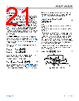
21 / 27 page  Data Sheet AD8027/AD8028 THEORY OF OPERATION analog.com Rev. E | 21 of 27 OUTPUT STAGE The AD8027/AD8028 use a common emitter output structure to achieve rail-to-rail output capability. The output stage is designed to drive 50 mA of linear output current, 40 mA within 200 mV of the rail, and 2.5 mA within 35 mV of the rail. Loading of the output stage, including any possible feedback network, lowers the open-loop gain of the amplifier. Refer to Figure 53 for the loading behavior. Capacitive load can degrade the phase margin of the amplifier. The AD8027/AD8028 can drive up to 20 pF, G = +1, as shown in Figure 14. Include a small (25 Ω to 50 Ω) series resistor, RSNUB, if the capacitive load is to exceed 20 pF for a gain of 1. Increasing the closed-loop gain increases the amount of capacitive load that can be driven before a series resistor must be included. DC ERRORS The AD8027/AD8028 use two complementary input stages to ach- ieve rail-to-rail input performance, as described in the Input Stage section. To use the dc performance over the entire common-mode range, the input bias current and input offset voltage of each pair must be considered. Referring to Figure 61, the output offset voltage of each pair is calculated by VOS,PNP,OUT=VOS,PNP RG+RFRG VOS,NPN,OUT=VOS,NPN RG+RFRG (4) where the difference of the two input stages is the discontinuity experienced when going through the crossover region. The size of the discontinuity is defined as VDIS= VOS,PNP−VOS,NPN × RG+RFRG (5) Using the crossover select feature of the AD8027/AD8028 helps to avoid this region. In the event that the region cannot be avoided, the quantity (VOS, PNP − VOS, NPN) is trimmed to minimize this effect. Because the input pairs are complementary, the input bias current reverses polarity when going through the crossover region shown in Figure 41. The offset between pairs is described by VOS,PNP−VOS,NPN= IB,PNP−IB,NPN × RS RG+RFRG −RF (6) where: IB, PNP is the input bias current of either input when the PNP input pair is active. IB, NPN is the input bias current of either input pair when the NPN pair is active. If RS is sized so that it equals RF when multiplied by the gain factor, this effect is eliminated. It is strongly recommended to balance the impedances in this manner when traveling through the crossover region to minimize the dc error and distortion. As an example, assuming that the PNP input pair has an input bias current of 6 µA and the NPN input pair has an input bias current of −2 µA, a 200 µV shift in offset occurs when traveling through the crossover region with RF equal to 0 Ω and RS equal to 25 Ω. In addition to the input bias current shift between pairs, each input pair has an input bias current offset that contributes to the total offset in the following manner: ∆VOS=IB+RS RG+RFRG −IB−RF (7) Figure 61. Op Amp DC Error Sources |
|
|
链接网址 |
| ALLDATASHEET是否为您带来帮助? [ DONATE ] |
关于 Alldatasheet | 广告服务 | 联系我们 | 隐私政策 | 数据表链接 | 链接交换 | 制造商名单 All Rights Reserved©Alldatasheet.com |
| Russian : Alldatasheetru.com | Korean : Alldatasheet.co.kr | Spanish : Alldatasheet.es | French : Alldatasheet.fr | Italian : Alldatasheetit.com Portuguese : Alldatasheetpt.com | Polish : Alldatasheet.pl | Vietnamese : Alldatasheet.vn Indian : Alldatasheet.in | Mexican : Alldatasheet.com.mx | British : Alldatasheet.co.uk | New Zealand : Alldatasheet.co.nz |
|
Family Site : ic2ic.com |
icmetro.com |
 Chinese ▼
 English
 Chinese
 German
 Japanese
 Russian
 Korean
 Spanish
 French
 Italian
 Portuguese
 Polish
 Vietnamese
 Indian
 Mexican
 British
 New Zealand