|
数据搜索系统,热门电子元器件搜索 |
|
|
数据搜索系统,热门电子元器件搜索 |
|
AD8027ARTZ-R2 数据表(PDF) 24 Page - Analog Devices |
|
|
|||||||||||||||||||||||||||||
AD8027ARTZ-R2 数据表(HTML) 24 Page - Analog Devices |
|
|
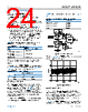
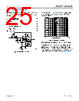
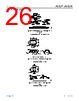
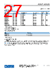
24 / 27 page  Data Sheet AD8027/AD8028 APPLICATIONS INFORMATION analog.com Rev. E | 24 of 27 USING THE DISABLE/SELECT PIN The AD8027/AD8028 unique DISABLE/SELECT pin has two func- tions: ► The power-down function places the AD8027/AD8028 into low power consumption mode. In power-down mode, the amplifiers draw 500 µA maximum of supply current. ► The second function, as described in the Crossover Selection section, shifts the crossover point (where the NPN/PNP input differential pairs transition from one to the other) closer to either the positive supply rail or the negative supply rail. This selectable crossover point allows the user to minimize distortion based on the input signal and environment. The default state is −1.2 V from the positive power supply, with the DISABLE/SELECT pin left floating or in tristate mode. In tristate mode, it is important that current to the pin is limited to ±20 μA maximum. Table 10 lists the voltage levels and modes of operation for the DISABLE/SELECT pin over the full temperature range. Table 10. DISABLE/SELECT Pin Mode Control Mode DISABLE/SELECT Pin Voltage (V) Disable −VS to –VS + 0.4 Crossover Referenced −1.2 V to Positive Supply −VS + 1.1 to –VS +1.3 Crossover Referenced +1.2 V to Negative Supply −VS + 2.0 to +VS When the input stage transitions from one input differential pair to the other, there is virtually no noticeable change in the output waveform. The disable time of the AD8027/AD8028 amplifiers is load depend- ent. Table 11 lists typical enable/disable times. See Figure 56 and Figure 57 for the actual switching measurements. Table 11. DISABLE/SELECT Switching Speeds Time Supply Voltages (RL = 1 kΩ) ±5 V +5 V +3 V tON 45 ns 50 ns 50 ns tOFF 980 ns 1100 ns 1150 ns DRIVING A 16-BIT ADC With the adjustable crossover distortion selection point and low noise, the AD8028 is an ideal amplifier for driving or buffering input signals into high resolution ADCs such as the AD7677, a 16-bit, 1 LSB INL, 1 MSPS differential ADC. Figure 65 shows the typical schematic for driving the ADC. The AD8028 driving the AD7677 offers performance close to nonrail-to-rail amplifiers and avoids the need for an additional supply other than the single 5 V supply already used by the ADC. In this application, the DISABLE/SELECT pins are biased to avoid the crossover region of the AD8028 for low distortion operation. Table 12 lists summary test data for the schematic shown in Figure 65. Table 12. ADC Driver Performance, fC = 100 kHz, VOUT = 4.7 V p-p Parameter Measurement Second Harmonic Distortion −105 dB Third Harmonic Distortion −102 dB Total Harmonic Distortion −102 dB SFDR 105 dBc Figure 65. Unity-Gain Differential Drive As shown in Figure 66, the AD8028 and AD7677 combination offers excellent integral nonlinearity (INL). Figure 66. Integral Nonlinearity BAND-PASS FILTER In communication systems, active filters are used extensively in signal processing. The AD8027/AD8028 are excellent choices for active filter applications. In realizing this filter, it is important that the amplifier have a large signal bandwidth of at least 10× the center frequency, fO. Otherwise, a phase shift can occur in the amplifier, causing instability and oscillations. In Figure 67, the AD8027/AD8028 device is configured as a 1 MHz band-pass filter. The target specifications are fO = 1 MHz and a −3 |
|
|
链接网址 |
| ALLDATASHEET是否为您带来帮助? [ DONATE ] |
关于 Alldatasheet | 广告服务 | 联系我们 | 隐私政策 | 数据表链接 | 链接交换 | 制造商名单 All Rights Reserved©Alldatasheet.com |
| Russian : Alldatasheetru.com | Korean : Alldatasheet.co.kr | Spanish : Alldatasheet.es | French : Alldatasheet.fr | Italian : Alldatasheetit.com Portuguese : Alldatasheetpt.com | Polish : Alldatasheet.pl | Vietnamese : Alldatasheet.vn Indian : Alldatasheet.in | Mexican : Alldatasheet.com.mx | British : Alldatasheet.co.uk | New Zealand : Alldatasheet.co.nz |
|
Family Site : ic2ic.com |
icmetro.com |
 Chinese ▼
 English
 Chinese
 German
 Japanese
 Russian
 Korean
 Spanish
 French
 Italian
 Portuguese
 Polish
 Vietnamese
 Indian
 Mexican
 British
 New Zealand