|
数据搜索系统,热门电子元器件搜索 |
|
|
数据搜索系统,热门电子元器件搜索 |
|
AD8067ART-R2 数据表(PDF) 20 Page - Analog Devices |
|
|
|||||||||||||||||||||||||||||
AD8067ART-R2 数据表(HTML) 20 Page - Analog Devices |
|
|
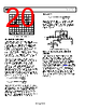
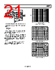
20 / 24 page  AD8067 Data Sheet Rev. B | Page 20 of 24 M 50ns CH1 288mV CH1 200mV CH2 200mV T VIN VOUT Figure 55. Gain of 3 Pulse Response SINGLE-SUPPLY OPERATION The AD8067 is well suited for low voltage single-supply applications, given its N-channel JFET input stage and rail-to- rail output stage. It is fully specified for 5 V supplies. Successful single-supply applications require attention to keep signal voltages within the input and output headroom limits of the amplifier. The input stage headroom extends to 1.7 V (minimum) on a 5 V supply. The center of the input range is 0.85 V. The output saturation limit defines the hard limit of the output headroom. This limit depends on the amount of current the amplifier is sourcing or sinking, as shown in Figure 29. Traditionally, an offset voltage is introduced in the input network replacing ground as a reference. This allows the output to swing about a dc reference point, typically midsupply. Attention to the required headroom of the amplifier is important, in this case, the required headroom from the positive supply is 3 V; therefore, 1.5 V was selected as a reference, which allows for a 100 mV signal at the input. Figure 56 shows the AD8067 configured for 5 V supply operation with a reference voltage of 1.5 V. Capacitors C1 and C5 ac couple the signal into and out of the amplifier and partially determine the bandwidth of the input and output structures. R1C1 Bandwidth dB 3 – VINPUT π = 2 1 C5 R Bandwidth dB 3 – V L OUTPUT π = 2 1 Resistors R2 and R3 set a 1.5 V output bias point for the output signal to swing about. It is critical to have adequate bypassing to provide a good ac ground for the reference voltage. Generally, the bandwidth of the reference network (R2, R3, and C2) is selected to be one tenth that of the input bandwidth. This ensures that any frequencies below the input bandwidth do not pass through the reference network into the amplifier. Reference network: ( )C2 R3 R2 Bandwidth dB 3 V REF || 2 1 π = − + Resistors R4 and R1 set the gain, in this case, an inverting gain of 10 was selected. In this application, the input and output bandwidths were set for approximately 10 Hz. The reference network was set for a tenth of the input and output bandwidth, at approximately 1 Hz. AD8067 C4 0.1 µF C3 10 µF +5V R4 2.7k Ω R1 300 Ω R3 30k Ω R2 70k Ω RL 1k Ω C5 15 µF VOUT 1 2 3 4 5 VIN C1 47 µF C2 6.8 µF +5V Figure 56. Single-Supply Operation Schematic HIGH GAIN, HIGH BANDWIDTH COMPOSITE AMPLIFIER The composite amplifier takes advantage of combining key parameters that can otherwise be mutually exclusive of a conventional single amplifier. For example, most precision amplifiers have good dc characteristics but lack high speed ac characteristics. Composite amplifiers combine the best of both amplifiers to achieve superior performance over their single op amp counterparts. The AD8067 and the AD8009 are well suited for a composite amplifier circuit, combining dc precision with high gain and bandwidth. The circuit runs off a ±5 V power supply at approximately 20 mA of bias current. With a gain of approximately 40 dB, the composite amplifier offers <1 pA input current, a gain bandwidth product of 6.1 GHz, and a slew rate of 630 V/µs. |
|
|
链接网址 |
| ALLDATASHEET是否为您带来帮助? [ DONATE ] |
关于 Alldatasheet | 广告服务 | 联系我们 | 隐私政策 | 数据表链接 | 链接交换 | 制造商名单 All Rights Reserved©Alldatasheet.com |
| Russian : Alldatasheetru.com | Korean : Alldatasheet.co.kr | Spanish : Alldatasheet.es | French : Alldatasheet.fr | Italian : Alldatasheetit.com Portuguese : Alldatasheetpt.com | Polish : Alldatasheet.pl | Vietnamese : Alldatasheet.vn Indian : Alldatasheet.in | Mexican : Alldatasheet.com.mx | British : Alldatasheet.co.uk | New Zealand : Alldatasheet.co.nz |
|
Family Site : ic2ic.com |
icmetro.com |
 Chinese ▼
 English
 Chinese
 German
 Japanese
 Russian
 Korean
 Spanish
 French
 Italian
 Portuguese
 Polish
 Vietnamese
 Indian
 Mexican
 British
 New Zealand