|
数据搜索系统,热门电子元器件搜索 |
|
|
数据搜索系统,热门电子元器件搜索 |
|
ADA4870ACPZ-R7 数据表(PDF) 22 Page - Analog Devices |
|
|
|||||||||||||||||||||||||||||
ADA4870ACPZ-R7 数据表(HTML) 22 Page - Analog Devices |
|
|
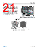
22 / 24 page  Data Sheet ADA4870 APPLICATIONS INFORMATION analog.com Rev. B | 22 of 24 PRINTED CIRCUIT BOARD (PCB) All current feedback amplifiers, including the ADA4870, can be affected by stray capacitance. Paying careful attention during PCB layout can reduce parasitic capacitance and improve overall circuit performance. Minimize signal trace lengths by placing feedback and gain setting resistors as close as possible to the amplifier. Additionally, for high output current amplifiers like the ADA4870, lay out the PCB with heat dissipation in mind. A good thermal design includes an exposed copper landing area on the top side of the board on which to solder the exposed pad of the LFCSP package. The PCB should also provide an exposed copper area on the bottom side to accommodate a heat sink. Stitch the top and bottom layers together with an array of plated-through thermal vias to facilitate efficient heat transfer through the board. Thermal conductivity may be further improved by using widely available via fill materials. THERMAL MODELING Computational fluid dynamics (CFD) tools like FloTherm® can be used to create layers of materials that include PCB construction, thermal vias, thermal interface materials, and heat sinks, and can predict junction temperature and/or junction to ambient thermal resistance (θJA) for a given set of conditions. Table 7 shows an example of how θJA is affected by the addition of an aluminum heat sink and forced convection. Figure 76 shows an image of the model used to establish the thermal results in Table 7. Figure 76. Thermal Model Stack-Up for Data in Table 7 (Heat Sink Not Shown) HEAT SINK SELECTION A heat sink increases the surface area to ambient temperature (TA) and extends the power dissipation capability of the ADA4870 and PCB combination. To maximize heat transfer from the board to the heat sink, attach the heat sink to the PCB using a high conductivity thermal interface material (TIM). The heat sink presented in the Safe Operating Area section and Figure 74 is effective up to ~10 W in still air. If lower power dissipation is anticipated and/or forced air convection is used, a smaller heat sink may be appropriate. If the thermal resistance of the chip (θJC), PCB (θCB), and TIM (θTIM) are known, use Equation 3 to compute the thermal resistance (θHS) of the required heat sink. θHS= TJ–TAPDISS – θJC+θCB+θTIM (3) POWER SUPPLIES AND DECOUPLING The ADA4870 can operate from a single supply or dual supplies. The total supply voltage (VCC − VEE) must be between 10 V and 40 V. Decouple each supply pin to ground using high quality, low ESR, 0.1 μF capacitors. Place decoupling capacitors as close to the supply pins as possible. Additionally, place 22 μF tantalum ca- pacitors from each supply to ground to provide good low frequency decoupling and supply the needed current to support large, fast slewing signals at the ADA4870 output. Table 7. Effects of Heat Sink and Forced Convection on θJA Heat Sink Dimensions, L × W × Total Height (mm) Heat Sink Base Thickness (mm) No. of Fins Air Flow (m/sec) θJA (°C/W) at TA = 25°C 61 × 58, Exposed Copper on Board, No Heat Sink Not applicable Not applicable 0 16.3 61 × 58, Exposed Copper on Board, No Heat Sink Not applicable Not applicable 2.73 11.43 61 × 58 × 24 2.29 8 0 9.94 61 × 58 × 24 2.29 8 2.73 7.26 |
|
|
链接网址 |
| ALLDATASHEET是否为您带来帮助? [ DONATE ] |
关于 Alldatasheet | 广告服务 | 联系我们 | 隐私政策 | 数据表链接 | 链接交换 | 制造商名单 All Rights Reserved©Alldatasheet.com |
| Russian : Alldatasheetru.com | Korean : Alldatasheet.co.kr | Spanish : Alldatasheet.es | French : Alldatasheet.fr | Italian : Alldatasheetit.com Portuguese : Alldatasheetpt.com | Polish : Alldatasheet.pl | Vietnamese : Alldatasheet.vn Indian : Alldatasheet.in | Mexican : Alldatasheet.com.mx | British : Alldatasheet.co.uk | New Zealand : Alldatasheet.co.nz |
|
Family Site : ic2ic.com |
icmetro.com |
 Chinese ▼
 English
 Chinese
 German
 Japanese
 Russian
 Korean
 Spanish
 French
 Italian
 Portuguese
 Polish
 Vietnamese
 Indian
 Mexican
 British
 New Zealand