|
数据搜索系统,热门电子元器件搜索 |
|
|
数据搜索系统,热门电子元器件搜索 |
|
AD8002ARZ-R7 数据表(PDF) 14 Page - Analog Devices |
|
|
|||||||||||||||||||||||||||||
AD8002ARZ-R7 数据表(HTML) 14 Page - Analog Devices |
|
|
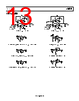
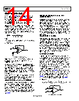
14 / 21 page  AD8002 Data Sheet Rev. E | Page 14 of 21 THEORY OF OPERATION An analysis of the AD8002 can put the operation in familiar terms. The open-loop behavior of the AD8002 is expressed as transimpedance, ΔVOUT/ΔI−INx, or TZ. The open-loop transimpedance behaves just as the open-loop voltage gain of a voltage feedback amplifier, that is, it has a large dc value and decreases at roughly 6 dB/octave in frequency. Because the value of RIN is proportional to 1/gm, the equivalent voltage gain is just TZ × gm, where the gm in question is the transconductance of the input stage. This results in a low open- loop input impedance at the inverting input. Using this amplifier as a follower with gain (see Figure 48) basic analysis yields the following result: R1 R G s T s T G V V IN Z Z IN OUT + × + × = ) ( ) ( where: TZ(s) implies the transimpedance as a function of the frequency. G = 1 + R1/R2. RIN = 1/gm ≈ 50 Ω. VOUT R1 R2 RIN VIN Figure 48. Small Signal Schematic Recognizing that G × RIN << R1 for low gains, the amplifier can be seen to the first-order that the bandwidth for it is independent of gain (G). Considering that additional poles contribute excess phase at high frequencies, there is a minimum feedback resistance below which peaking or oscillation may result. This fact is used to determine the optimum feedback resistance, RF. In practice, parasitic capacitance at the inverting input terminal also adds phase in the feedback loop; thus selecting an optimum value for RF can be difficult. Achieving and maintaining gain flatness of better than 0.1 dB at frequencies above 10 MHz requires careful consideration of several issues discussed in the following sections. CHOICE OF FEEDBACK AND GAIN RESISTORS The fine scale gain flatness varies to some extent with feedback resistance. Therefore, it is recommended that as soon as optimum resistor values are determined, use 1% tolerance values if it is desired to maintain flatness over a wide range of production lots. In addition, resistors of different construction have different associated parasitic capacitance of the character- ization. It is not recommended to use leaded components with the AD8002. PRINTED CIRCUIT BOARD (PCB) LAYOUT CONSIDERATIONS As expected for a wideband amplifier, PCB parasitics can affect the overall closed-loop performance. Of concern are stray capacitances at the output and the inverting input nodes. If a ground plane is to be used on the same side of the board as the signal traces, leave a space (5 mm minimum) around the signal lines to minimize coupling. Additionally, make signal lines connecting the feedback and gain resistors short enough so that their associated inductance does not cause high frequency gain errors. Line lengths of less than 5 mm are recommended. If long runs of coaxial cable are being driven, dispersion and loss must be considered. POWER SUPPLY BYPASSING Adequate power supply bypassing can be critical when optimiz- ing the performance of a high frequency circuit. Inductance in the power supply leads can form resonant circuits that produce peaking in the response of the amplifier. In addition, if large current transients must be delivered to the load, bypass capaci- tors (typically greater than 1 μF) are required to provide the best settling time and lowest distortion. A parallel combination of 4.7 μF and 0.1 μF is recommended. Some brands of electrolytic capacitors require a small series damping resistor ≈4.7 Ω for optimum results. DC ERRORS AND NOISE There are three major noise and offset terms to consider in a current feedback amplifier. For offset errors, refer to Equation 1. For noise error, the terms are root-sum-squared to give a net output error. In Figure 49, the terms are input offset (VIO), which appears at the output multiplied by the noise gain of the circuit (1 + RF/RI), noninverting input current (IBN × RN), also multiplied by the noise gain, and the inverting input current, which when divided between RF and RI and subsequently multiplied by the noise gain, always appears at the output as IBN × RF. The input voltage noise of the AD8002 is a low 2 nV/√Hz. At low gains, though, the inverting input current noise times RF is the dominant noise source. Careful layout and device matching contribute to a better offset and drift specifications for the AD8002.Use the typical performance curves in conjunction with Equation 1 to predict the performance of the AD8002 in any application. F BI I F N BN I F IO OUT R I R R R I R R V V × × + × × ± + × = 1 1 (1) RF RI RN IBN VOUT IBI Figure 49. Output Offset Voltage |
|
|
链接网址 |
| ALLDATASHEET是否为您带来帮助? [ DONATE ] |
关于 Alldatasheet | 广告服务 | 联系我们 | 隐私政策 | 数据表链接 | 链接交换 | 制造商名单 All Rights Reserved©Alldatasheet.com |
| Russian : Alldatasheetru.com | Korean : Alldatasheet.co.kr | Spanish : Alldatasheet.es | French : Alldatasheet.fr | Italian : Alldatasheetit.com Portuguese : Alldatasheetpt.com | Polish : Alldatasheet.pl | Vietnamese : Alldatasheet.vn Indian : Alldatasheet.in | Mexican : Alldatasheet.com.mx | British : Alldatasheet.co.uk | New Zealand : Alldatasheet.co.nz |
|
Family Site : ic2ic.com |
icmetro.com |
 Chinese ▼
 English
 Chinese
 German
 Japanese
 Russian
 Korean
 Spanish
 French
 Italian
 Portuguese
 Polish
 Vietnamese
 Indian
 Mexican
 British
 New Zealand