|
数据搜索系统,热门电子元器件搜索 |
|
|
数据搜索系统,热门电子元器件搜索 |
|
AD8002ARZ-R7 数据表(PDF) 18 Page - Analog Devices |
|
|
|||||||||||||||||||||||||||||
AD8002ARZ-R7 数据表(HTML) 18 Page - Analog Devices |
|
|
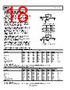
18 / 21 page  AD8002 Data Sheet Rev. E | Page 18 of 21 APPLICATIONS INFORMATION LAYOUT CONSIDERATIONS The specified high speed performance of the AD8002 requires careful attention to board layout and component selection. Proper RF design techniques and low parasitic component selection are mandatory. Use a ground plane to cover all unused portions of the component side of the board to provide a low impedance ground path. Remove the ground plane from the area near the input pins to reduce stray capacitance. Use chip capacitors for supply bypassing (see Figure 58). Connect one end to the ground plane and the other within ⅛ inch of each power pin. Connect an additional large tantalum electrolytic capacitor (4.7 µF to 10 µF) in parallel, but not necessarily so close, to supply current for fast, large signal changes at the output. Locate the feedback resistor close to the inverting input pin to keep the stray capacitance at this node to a minimum. Capacitance variations of less than 1 pF at the inverting input significantly affects high speed performance. Use stripline design techniques for long signal traces (greater than about 1 inch). Design these with a characteristic impedance of 50 Ω or 75 Ω and ensure they are properly terminated at each end. Table 4 and Table 5 show the recommended component values. RF RBT IN –VS +VS RS RT RG OUT Figure 57. Inverting Configuration C1 0.1µF C3 10µF C2 0.1µF C4 10µF +VS –VS Figure 58. Supply Bypassing RF RBT IN –VS +VS RT RG OUT RC Figure 59. Noninverting Configuration Table 4. AD8002AR (SOIC) Recommended Component Values1 Component Gain Unit −10 −2 −1 +1 +2 +10 +100 RF 499 499 549 953 681 499 1000 Ω RG 49.9 249 549 N/A 681 54.9 10 Ω RBT (Nominal) 49.9 49.9 49.9 49.9 49.9 49.9 49.9 Ω RC2 N/A N/A N/A 75 75 0 0 Ω RS 49.9 49.9 49.9 N/A N/A N/A N/A Ω RT (Nominal) N/A 61.9 54.9 49.9 49.9 49.9 49.9 Ω Small Signal Bandwidth 250 410 410 600 500 170 17 MHz 0.1 dB Flatness 50 100 100 35 90 24 3 MHz 1 N/A means not applicable 2 RC is recommended to reduce peaking, and minimizes input reflections at frequencies above 300 MHz. However, RC is not required. Table 5. AD8002ARM (MSOP) Recommended Component Values1 Component Gain Unit −10 −2 −1 +1 +2 +10 +100 RF 499 499 590 1000 681 499 1000 Ω RG 49.9 249 590 N/A 681 54.9 10 Ω RBT (Nominal) 49.9 49.9 49.9 49.9 49.9 49.9 49.9 Ω RC2 N/A N/A N/A 75 75 0 0 Ω RS 49.9 49.9 49.9 N/A N/A N/A N/A Ω RT (Nominal) N/A 61.9 49.9 49.9 49.9 49.9 49.9 Ω Small Signal Bandwidth 270 400 410 600 450 170 19 MHz 0.1 dB Flatness 60 100 100 35 70 35 3 MHz 1 N/A means not applicable 2 RC is recommended to reduce peaking, and minimizes input reflections at frequencies above 300 MHz. However, RC is not required. |
|
|
链接网址 |
| ALLDATASHEET是否为您带来帮助? [ DONATE ] |
关于 Alldatasheet | 广告服务 | 联系我们 | 隐私政策 | 数据表链接 | 链接交换 | 制造商名单 All Rights Reserved©Alldatasheet.com |
| Russian : Alldatasheetru.com | Korean : Alldatasheet.co.kr | Spanish : Alldatasheet.es | French : Alldatasheet.fr | Italian : Alldatasheetit.com Portuguese : Alldatasheetpt.com | Polish : Alldatasheet.pl | Vietnamese : Alldatasheet.vn Indian : Alldatasheet.in | Mexican : Alldatasheet.com.mx | British : Alldatasheet.co.uk | New Zealand : Alldatasheet.co.nz |
|
Family Site : ic2ic.com |
icmetro.com |
 Chinese ▼
 English
 Chinese
 German
 Japanese
 Russian
 Korean
 Spanish
 French
 Italian
 Portuguese
 Polish
 Vietnamese
 Indian
 Mexican
 British
 New Zealand