|
数据搜索系统,热门电子元器件搜索 |
|
|
数据搜索系统,热门电子元器件搜索 |
|
AD8002ARZ-R7 数据表(PDF) 17 Page - Analog Devices |
|
|
|||||||||||||||||||||||||||||
AD8002ARZ-R7 数据表(HTML) 17 Page - Analog Devices |
|
|
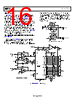
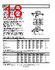
17 / 21 page  Data Sheet AD8002 Rev. E | Page 17 of 21 The current feedback nature of the op amps, in addition to enabling the wide bandwidth, provides an output drive of more than 3 V p-p into a 20 Ω load for each output at 20 MHz. Conversely, the voltage feedback nature provides symmetrical high impedance inputs and allows the use of reactive components in the feedback network. The circuit consists of the two op amps, each configured as a unity-gain follower by the 511 Ω RA feedback resistors between the output and inverting input of each op amp. The output of each op amp has a 511 Ω RB resistor to the inverting input of the other op amp. Thus, each output drives the other op amp through a unity-gain inverter configuration. By connecting the two amplifiers as cross-coupled inverters, the outputs of the amplifiers are freed to be equal and opposite, assuring zero output common-mode voltage. Using this circuit configuration, the common-mode signal of the outputs is reduced. If one output increases slightly, the negative input to the other op amp drives its output slightly lower and thus preserves the symmetry of the complementary outputs, which reduces the common-mode signal. The common- mode output signal was measured as −50 dB at 1 MHz. Looking at this configuration overall, there are two high impedance inputs (the +IN1, +IN2 of each op amp), two low impedance outputs, and a high open-loop gain. The two noninverting inputs and the output of the Op Amp 2 structure looks like a voltage feedback op amp having two symmetrical, high impedance inputs and one output. The +IN1, +IN2 to Op Amp 2 is the noninverting input (it has the same polarity as OUT2) and the +IN1, +IN2 to Op Amp 1 is the inverting input (opposite polarity of Output 2). With a feedback resistor, RF, an input resistor, RG, and the grounding of the +IN1, +IN2 of Op Amp 2, a feedback amplifier is formed. This configuration is similar to a voltage feedback amplifier in an inverting configuration if only OUT2 is considered. The addition of OUT1 makes the amplifier a differential output. The differential gain of this circuit is + × = B A G F R R R R G 1 where: RF/RG is the gain of the overall op amp configuration and is the same as for an inverting op amp except for the polarity. If OUT1 is used as the output reference, the gain is positive. 1 + RA/RB is the noise gain of each individual op amp in its noninverting configuration. The resulting architecture offers several advantages. First, the gain can be changed by changing a single resistor. Changing either RF or RG changes the gain as in an inverting op amp circuit. For most types of differential circuits, more than one resistor must be changed to change gain and still maintain good common-mode rejection (CMR). Reactive elements can be used in the feedback network. This is in contrast to current feedback amplifiers that restrict the use of reactive elements in the feedback op amp. The circuit described requires about 0.9 pF of capacitance in shunt across RF to optimize peaking and realize a −3 dB bandwidth of more than 200 MHz. The peaking exhibited by the circuit is very sensitive to the value of this capacitor. Parasitics in the board layout on the order of tenths of picofarads influences the frequency response and the value required for the feedback capacitor, thus a good layout is essential. The shunt capacitor type selection is also critical. A good microwave type chip capacitor with high Q was found to yield best performance. The device selected for this circuit was a Murata Erie MA280R9B. The distortion was measured at 20 MHz with a 3 V p-p input and a 100 Ω load on each output. For OUT1, the distortion is −37 dBc and −41 dBc for the second and third harmonics, respectively. For OUT2, the second harmonic is −35 dBc and the third harmonic is −43 dBc. 6 –4 –14 1G 10M 1M 100M –6 –8 –10 –12 –2 0 2 4 FREQUENCY (Hz) CC = 0.9pF OUT+ OUT– Figure 56. Differential Driver Frequency Response |
|
|
链接网址 |
| ALLDATASHEET是否为您带来帮助? [ DONATE ] |
关于 Alldatasheet | 广告服务 | 联系我们 | 隐私政策 | 数据表链接 | 链接交换 | 制造商名单 All Rights Reserved©Alldatasheet.com |
| Russian : Alldatasheetru.com | Korean : Alldatasheet.co.kr | Spanish : Alldatasheet.es | French : Alldatasheet.fr | Italian : Alldatasheetit.com Portuguese : Alldatasheetpt.com | Polish : Alldatasheet.pl | Vietnamese : Alldatasheet.vn Indian : Alldatasheet.in | Mexican : Alldatasheet.com.mx | British : Alldatasheet.co.uk | New Zealand : Alldatasheet.co.nz |
|
Family Site : ic2ic.com |
icmetro.com |
 Chinese ▼
 English
 Chinese
 German
 Japanese
 Russian
 Korean
 Spanish
 French
 Italian
 Portuguese
 Polish
 Vietnamese
 Indian
 Mexican
 British
 New Zealand