|
数据搜索系统,热门电子元器件搜索 |
|
|
数据搜索系统,热门电子元器件搜索 |
|
ADL5902ACPZ-R7 数据表(PDF) 20 Page - Analog Devices |
|
|
|||||||||||||||||||||||||||||
ADL5902ACPZ-R7 数据表(HTML) 20 Page - Analog Devices |
|
|
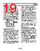
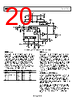
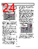
20 / 28 page  ADL5902 Data Sheet Rev. B | Page 20 of 28 X2 X2 BIAS AND POWER- DOWN CONTROL 1 NC NC NC LINEAR-IN-dB VGA (NEGATIVE SLOPE) IDET 26pF 2 3 4 11 10 9 5 6 7 8 16 15 14 13 ADL5902 12 VREF 2.3V TEMPERATURE SENSOR INLO INHI VPOS POS TEMP (BLACK) GND (BLACK) VSET (BLACK) VOUT (BLACK) VTGT (BLACK) VREF (BLACK) TEMP VSET VOUT CLPF COMM COMM VTGT VREF TADJ/PWDN G = 5 ITGT R3 60.4Ω C10 100pF C12 100pF VPOS +5V (RED) C4 100pF C3 0.1µF C5 100pF C7 0.1µF R11 2kΩ R10 3.74kΩ R12 301Ω R9 1430Ω C9 10µF RFIN R2 OPEN R6 0Ω R1 0Ω R15 OPEN TC2 PWDN (BLACK) Figure 45. Basic Connections for Operation in Measurement Mode SETTING VTADJ As discussed in the Theory of Operation section, the output temperature drift must be compensated by applying a voltage to the TADJ pin. The compensating voltage varies with frequency. The voltage for the TADJ pin can be easily derived from a resistor divider connected to the VREF pin. Table 5 shows the recom- mended VTADJ for operation from −40°C to +85°C, along with resistor divider values. Resistor values are chosen so that they neither pull too much current from VREF (VREF short-circuit current is 4 mA) nor are so large that the TADJ pin bias current of 3 μA affects the resulting voltage at the TADJ pin. Table 5. Recommended VTADJ for Selected Frequencies Frequency VTADJ (V) R9 (Ω) R12 (Ω) 100 MHz 0.5 1430 402 700 MHz to 2.14 GHz 0.4 1430 301 2.6 GHz 0.45 1430 348 3.5 GHz 0.5 1430 402 5.8 GHz 0.95 1430 1007 SETTING VTGT As discussed in the Theory of Operation section, setting the voltage on VTGT to 0.8 V represents a compromise between achieving excellent rms compliance and maximizing dynamic range. The voltage on VTGT can be derived from the VREF pin using a resistor divider as shown Figure 45 (Resistor R10 and Resistor R11). Like the resistors chosen to set the VTADJ voltage, the resistors setting VTGT must have reasonable values that do not pull too much current from VREF or cause bias current errors. Also, attention must be paid to the combined current that VREF must deliver to generate the VTADJ and VTGT voltages. This current must be kept well below the VREF short-circuit current of 4 mA. CHOOSING A VALUE FOR CLPF CLPF (C9 in Figure 45) provides the averaging function for the internal rms computation. Using the minimum value for CLPF allows the quickest response time to a pulsed waveform but leaves significant output noise on the output voltage signal. By the same token, a large filter cap reduces output noise but at the expense of response time. For non response-time critical applications, a relatively large capacitor can be placed on the CLPF pin. In Figure 45, a value of 0.1 μF is used. For most signal modulation schemes, this value ensures excellent rms measurement compliance and low residual output noise. There is no maximum capacitance limit for CLPF. |
|
|
链接网址 |
| ALLDATASHEET是否为您带来帮助? [ DONATE ] |
关于 Alldatasheet | 广告服务 | 联系我们 | 隐私政策 | 数据表链接 | 链接交换 | 制造商名单 All Rights Reserved©Alldatasheet.com |
| Russian : Alldatasheetru.com | Korean : Alldatasheet.co.kr | Spanish : Alldatasheet.es | French : Alldatasheet.fr | Italian : Alldatasheetit.com Portuguese : Alldatasheetpt.com | Polish : Alldatasheet.pl | Vietnamese : Alldatasheet.vn Indian : Alldatasheet.in | Mexican : Alldatasheet.com.mx | British : Alldatasheet.co.uk | New Zealand : Alldatasheet.co.nz |
|
Family Site : ic2ic.com |
icmetro.com |
 Chinese ▼
 English
 Chinese
 German
 Japanese
 Russian
 Korean
 Spanish
 French
 Italian
 Portuguese
 Polish
 Vietnamese
 Indian
 Mexican
 British
 New Zealand