|
数据搜索系统,热门电子元器件搜索 |
|
|
数据搜索系统,热门电子元器件搜索 |
|
ADL5906ACPZN-R7 数据表(PDF) 23 Page - Analog Devices |
|
|
|||||||||||||||||||||||||||||
ADL5906ACPZN-R7 数据表(HTML) 23 Page - Analog Devices |
|
|
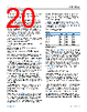
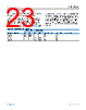
23 / 30 page  Data Sheet ADL5906 THEORY OF OPERATION analog.com Rev. B | 23 of 30 VSET. Therefore, the values for R6 and R2 must be in the 1 kΩ to 5 kΩ range. Similar values must be used for R1 and R15. It is also important to take into account part-to-part and frequency variation in output swing along with the maximum output voltage (3.9 V) of the output stage of the ADL5906. The VRMS part-to-part distribution is well characterized at major frequency bands in the Typical Performance Characteristics section (see Figure 12 through Figure 14, Figure 18 through Figure 20, Figure 24, and Figure 25). The resistor values in Table 6, which were calculated based on 3.5 GHz operation, have been conservatively chosen so that there is no chance that the desired output voltage swings exceed the output swing of the ADL5906 (when scaling upward) or the input range of a 0 V to 2.5 V ADC (when scaling down-ward). In each case, the nominal maximum voltage that results is 100 mV below the desired maximum to account for part-to-part variation and resistor tolerances. Table 6. Output Voltage Range Scaling Examples at 3.5 GHz Desired Input Range (dBm) Slope Increase Slope Decrease New Slope (mV/dB) Nominal Maximum Output Voltage (V) R6 (Ω) R2 (Ω) R1 (Ω) R15(Ω) 0 to −60 274 2000 59 3.8 −10 to −50 681 2000 70 3.8 0 to −60 787 2000 37 2.4 −10 to −50 348 2000 44 2.4 |
|
|
链接网址 |
| ALLDATASHEET是否为您带来帮助? [ DONATE ] |
关于 Alldatasheet | 广告服务 | 联系我们 | 隐私政策 | 数据表链接 | 链接交换 | 制造商名单 All Rights Reserved©Alldatasheet.com |
| Russian : Alldatasheetru.com | Korean : Alldatasheet.co.kr | Spanish : Alldatasheet.es | French : Alldatasheet.fr | Italian : Alldatasheetit.com Portuguese : Alldatasheetpt.com | Polish : Alldatasheet.pl | Vietnamese : Alldatasheet.vn Indian : Alldatasheet.in | Mexican : Alldatasheet.com.mx | British : Alldatasheet.co.uk | New Zealand : Alldatasheet.co.nz |
|
Family Site : ic2ic.com |
icmetro.com |
 Chinese ▼
 English
 Chinese
 German
 Japanese
 Russian
 Korean
 Spanish
 French
 Italian
 Portuguese
 Polish
 Vietnamese
 Indian
 Mexican
 British
 New Zealand