|
数据搜索系统,热门电子元器件搜索 |
|
|
数据搜索系统,热门电子元器件搜索 |
|
AD8318ACPZ-R2 数据表(PDF) 18 Page - Analog Devices |
|
|
|||||||||||||||||||||||||||||
AD8318ACPZ-R2 数据表(HTML) 18 Page - Analog Devices |
|
|
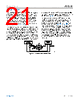
18 / 24 page  Data Sheet AD8318 USING THE AD8318 analog.com Rev. E | 18 of 24 Figure 39. AD8318 Operating with the High Speed ADCMP563 Comparator RESPONSE TIME CAPABILITY The AD8318 has a 10 ns rise/fall time capability (10% to 90%) for input power switching between the noise floor and 0 dBm. This capability enables RF burst measurements at repetition rates beyond 45 MHz. In most measurement applications, the AD8318 has an external capacitor connected to CLPF to provide additional filtering for VOUT. However, using the CLPF capacitor slows the response time as does stray capacitance on VOUT. For an applica- tion requiring maximum RF burst detection capability, the CLPF pin is left unconnected. In this case, the integration function is provided by the 1.5 pF on-chip capacitor. There is a 10 Ω internal resistor in series with the output driver. Because of this resistor, it is necessary to add an external 40 Ω back-terminating resistor in series with the output when driving a 50 Ω load. Place the back-terminating resistor close to the VOUT pin. The AD8318 has the drive capability to drive a 50 Ω load at the end of a coaxial cable or transmission line when back terminated (see Figure 39). The circuit diagram in Figure 39 shows the AD8318 used with a high speed comparator circuit. The 40 Ω series resistor at the output of the AD8318 combines with an internal 10 Ω to properly match to the 50 Ω input of the comparator. Figure 40. Pulse Response of AD8318 and Comparator for RF Pulses of Varying Amplitudes Figure 40 shows the response of the AD8318 and the comparator for a 500 MHz pulsed sine wave of varying amplitudes. The output level of the AD8318 is the signal strength of the input signal. For applications where these RF bursts are very small, the output level does not change by a large amount. Using a comparator is beneficial in this case because it turns the output of the log amp into a limiter-like signal. While this configuration does result in the loss of received signal power level, it does allow for presence-only detection of low power RF bursts. OUTPUT FILTERING For applications in which maximum video bandwidth and, conse- quently, fast rise time are desired, it is essential that the CLPF pin be left unconnected and free of any stray capacitance. To reduce the nominal output video bandwidth of 45 MHz, connect a ground-referenced capacitor (CFLT) to the CLPF pin, as shown in Figure 41. Generally, this is done to reduce output ripple (at twice the input frequency for a symmetric input waveform, such as sinusoidal signals). Figure 41. Lowering the Postdemodulation Bandwidth CFLT is selected by CFLT= 1 π×3.13kΩ×VideoBandwidtℎ −1.5pF (19) Set the video bandwidth to a frequency equal to about one-tenth the minimum input frequency. This ensures that the output ripple of the demodulated log output, which is at twice the input frequency, is well filtered. In many log amp applications, it may be necessary to lower the corner frequency of the postdemodulation filtering to achieve low output ripple while maintaining a rapid response time to changes in signal level. For an example of a 4-pole active filter, see the AD8307 data sheet. CONTROLLER MODE The AD8318 provides a controller mode feature at the VOUT pin. Using VSET for the setpoint voltage, it is possible for the AD8318 to |
|
|
链接网址 |
| ALLDATASHEET是否为您带来帮助? [ DONATE ] |
关于 Alldatasheet | 广告服务 | 联系我们 | 隐私政策 | 数据表链接 | 链接交换 | 制造商名单 All Rights Reserved©Alldatasheet.com |
| Russian : Alldatasheetru.com | Korean : Alldatasheet.co.kr | Spanish : Alldatasheet.es | French : Alldatasheet.fr | Italian : Alldatasheetit.com Portuguese : Alldatasheetpt.com | Polish : Alldatasheet.pl | Vietnamese : Alldatasheet.vn Indian : Alldatasheet.in | Mexican : Alldatasheet.com.mx | British : Alldatasheet.co.uk | New Zealand : Alldatasheet.co.nz |
|
Family Site : ic2ic.com |
icmetro.com |
 Chinese ▼
 English
 Chinese
 German
 Japanese
 Russian
 Korean
 Spanish
 French
 Italian
 Portuguese
 Polish
 Vietnamese
 Indian
 Mexican
 British
 New Zealand