|
数据搜索系统,热门电子元器件搜索 |
|
|
数据搜索系统,热门电子元器件搜索 |
|
PPC405GPR-3JB400 数据表(PDF) 30 Page - Applied Micro Circuits Corporation |
|
|
|||||||||||||||||||||||||||||
PPC405GPR-3JB400 数据表(HTML) 30 Page - Applied Micro Circuits Corporation |
|
|
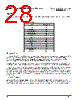
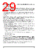
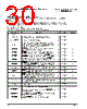
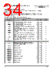
30 / 57 page  405GPr – Power PC 405GPr Embedded Processor 30 AMCC Revision 2.04 – September 7, 2007 Data Sheet Signal Functional Description (Sheet 1 of 8) Multiplexed signals are shown in brackets following the first signal name assigned to each multiplexed ball. Notes: 1. Receiver input has hysteresis. 2. Must pull up. See “Pull-Up and Pull-Down Resistors” on page 29 for recommended termination values. 3. Must pull down. See “Pull-Up and Pull-Down Resistors” on page 29 for recommended termination values. 4. If not used, must pull up. 5. If not used, must pull down. 6. Strapping input during reset; pull up or pull down as required. 7. Pull-up may be required. See “External Bus Control Signals” on page 29. Signal Name Description I/O Type Notes PCI Interface PCIAD31:0 PCI Address/Data Bus. Multiplexed address and data bus. I/O 5V tolerant 3.3V PCI PCIC3:0[BE3:0] PCI bus command and byte enables. I/O 5V tolerant 3.3V PCI PCIParity PCI parity. Parity is even across PCIAD0:31 and PCIC0:3[BE0:3]. PCIParity is valid one cycle after either an address or data phase. The PCI device that drove PCIAD0:31 is responsible for driving PCIParity on the next PCI bus clock. I/O 5V tolerant 3.3V PCI PCIFrame PCIFrame is driven by the current PCI bus master to indicate the beginning and duration of a PCI access. I/O 5V tolerant 3.3V PCI 2 PCIIRDY PCIIRDY is driven by the current PCI bus master. Assertion of PCIIRDY indicates that the PCI initiator is ready to transfer data. I/O 5V tolerant 3.3V PCI 2 PCITRDY The target of the current PCI transaction drives PCITRDY. Assertion of PCITRDY indicates that the PCI target is ready to transfer data. I/O 5V tolerant 3.3V PCI 2 PCIStop The target of the current PCI transaction can assert PCIStop to indicate to the requesting PCI master that it wants to end the current transaction. I/O 5V tolerant 3.3V PCI 2 PCIDevSel PCIDevSel is driven by the target of the current PCI transaction. A PCI target asserts PCIDevSel when it has decoded an address and command encoding and claims the transaction. I/O 5V tolerant 3.3V PCI 2 PCIIDSel PCIIDSel is used during configuration cycles to select the PCI slave interface for configuration. I 5V tolerant 3.3V PCI PCISErr PCISErr is used for reporting address parity errors or catastrophic failures detected by a PCI target. I/O 5V tolerant 3.3V PCI 2 PCIPErr PCIPErr is used for reporting data parity errors on PCI transactions. PCIPErr is driven active by the device receiving PCIAD0:31, PCIC0:3[BE0:3], and PCIParity, two PCI clocks following the data in which bad parity is detected. I/O 5V tolerant 3.3V PCI 2 PCIClk PCIClk is used as the asynchronous PCI clock when in asynchronous mode. It is unused when the PCI interface is operated synchronously with the PLB bus. I 5V tolerant 3.3V PCI PCIReset PCI specific reset. O 5V tolerant 3.3V PCI PCIINT[PerWE] PCI interrupt. Open-drain output (two states; 0 or open circuit) or Peripheral write enable. Low when any of the four PerWBE0:3 write byte enables are low. O 5V tolerant 3.3V PCI PCIReq0[Gnt] Multipurpose signal, used as PCIReq0 when internal arbiter is used, and as Gnt when external arbiter is used. I 5V tolerant 3.3V PCI PCIReq1:5 Used as PCIReq1:5 input when internal arbiter is used. I 5V tolerant 3.3V PCI |
|
链接网址 |
| ALLDATASHEET是否为您带来帮助? [ DONATE ] |
关于 Alldatasheet | 广告服务 | 联系我们 | 隐私政策 | 数据表链接 | 链接交换 | 制造商名单 All Rights Reserved©Alldatasheet.com |
| Russian : Alldatasheetru.com | Korean : Alldatasheet.co.kr | Spanish : Alldatasheet.es | French : Alldatasheet.fr | Italian : Alldatasheetit.com Portuguese : Alldatasheetpt.com | Polish : Alldatasheet.pl | Vietnamese : Alldatasheet.vn Indian : Alldatasheet.in | Mexican : Alldatasheet.com.mx | British : Alldatasheet.co.uk | New Zealand : Alldatasheet.co.nz |
|
Family Site : ic2ic.com |
icmetro.com |
 Chinese ▼
 English
 Chinese
 German
 Japanese
 Russian
 Korean
 Spanish
 French
 Italian
 Portuguese
 Polish
 Vietnamese
 Indian
 Mexican
 British
 New Zealand