|
数据搜索系统,热门电子元器件搜索 |
|
|
数据搜索系统,热门电子元器件搜索 |
|
STDRIVEG611Q 数据表(PDF) 14 Page - STMicroelectronics |
|
|
|||||||||||||||||||||||||||||
STDRIVEG611Q 数据表(HTML) 14 Page - STMicroelectronics |
|
|
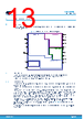
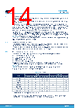
14 / 33 page  6.1.3 High-side driver This block receives input pulses from the logic section through the level shifter and provides driving action to the high-side GaN transistor. It is electrically referred to OUT, that must be connected to the source connection (preferably Kelvin) of the high- side GaN transistor. GaN VGS sink current can be tuned with the RGATE resistor placed between the OUTH and GaN gate. Source current can be tuned with the RON resistor between VCCH and RONH. Sink path impedance is the sum of RGATE and driver RSI, while source path impedance is the total of RON, RGATE and driver RSO. Tuning RON is typically done to adjust hard turn-on dV/dt. Tuning RGATE is typically done to eventually dump VGS ringing at turn-off, to adjust hard turn-off dV/dt while avoiding induced turn-on at low-side hard turn-on. High-side driver circuitry is supplied by the voltage present at the BOOT pin, while an integrated fast startup voltage regulator tightly stabilizes the supply voltage of the output stage of the driver (VHS). A UVLO comparator interrupts the high-side GaN activity if the regulator’s output voltage is insufficient for a proper GaN’s driving. See Section 6.4.4 for detailed HS UVLO protection description. This section includes an equivalent bootstrap diode, synchronous with low-side on-time, that generates floating supply voltage (VBO), starting from VCC voltage. 6.1.4 Comparator and smart shutdown The embedded comparator, typically used for overcurrent detection, immediately turns off both GaNs once CIN input exceeds the threshold. The event is signaled to SD/OD and FLT pins. The smart shutdown (SmartSD) feature allows to automatically keep the switches off for the desired time to cool down the GaN devices while the controller reacts to the overcurrent FLT signal. 6.2 Truth table and control inputs The STDRIVEG611 has four logic inputs to control the high-side and low-side power transistors. • LIN: low-side driver input, active high; • HIN: high-side driver inputs, active high. • STBY: standby input, active low; • SD/OD: shutdown input, active low. An open drain output is there (FLT) to communicate externally the operating status of the device. The SD/OD pin is also used as an output for the comparator with SmartSD disable time function (see Section 6.6). Table 6 summarizes the different IC operating modes depending on the Input pin configurations. Output pin configuration and IC consumption is also reported. Table 6. Truth table Mode INPUTS OUTPUTS STBY SD/OD LIN HIN OUTL OUTH FLT Standby L X X X L L L Shutdown H L X X L L H High-Z H H L L L L H Low-side on H H H L H L H High-side on H H L H L H H Interlocking H H H H L L H Overcurrent H L (1) X X L L L 1. Forced low from the internal open-drain when CIN > CINth. The logic inputs have internal pull-down resistors to set a defined logic level even in case of high-Z on signal lines. As a result, the transistors are set to off in the case of unconnected input pins. STDRIVEG611 Device description DS14457 - Rev 2 page 14/33 |
|
链接网址 |
| ALLDATASHEET是否为您带来帮助? [ DONATE ] |
关于 Alldatasheet | 广告服务 | 联系我们 | 隐私政策 | 数据表链接 | 链接交换 | 制造商名单 All Rights Reserved©Alldatasheet.com |
| Russian : Alldatasheetru.com | Korean : Alldatasheet.co.kr | Spanish : Alldatasheet.es | French : Alldatasheet.fr | Italian : Alldatasheetit.com Portuguese : Alldatasheetpt.com | Polish : Alldatasheet.pl | Vietnamese : Alldatasheet.vn Indian : Alldatasheet.in | Mexican : Alldatasheet.com.mx | British : Alldatasheet.co.uk | New Zealand : Alldatasheet.co.nz |
|
Family Site : ic2ic.com |
icmetro.com |
 Chinese ▼
 English
 Chinese
 German
 Japanese
 Russian
 Korean
 Spanish
 French
 Italian
 Portuguese
 Polish
 Vietnamese
 Indian
 Mexican
 British
 New Zealand