|
数据搜索系统,热门电子元器件搜索 |
|
|
数据搜索系统,热门电子元器件搜索 |
|
AP8012HSEC-R1 数据表(PDF) 6 Page - Wuxi Chipown Micro-electronics limited |
|
|
|||||||||||||||||||||||||||||
AP8012HSEC-R1 数据表(HTML) 6 Page - Wuxi Chipown Micro-electronics limited |
|
|
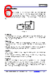
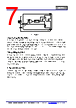
6 / 10 page  AP8012H 13/F, Building C, Wangzhuang Technology Innovation Center, Longshan Road,New District, Wuxi Tel: +86(510)85217718 http://www.chipown.com Rev.A 1801 6 / 10 Functional Description 1. Startup This device includes a high voltage start up current source connected on the SW of the device. As soon as a voltage is applied on the input of the converter, this start up current source is activated and to charge the VDD capacitor as long as VDD is lower than VSTART. When reaching VSTART, the start up current source is cut off and VDD is sourced by auxiliary side. As VDD falls below VSTOP, the HV-Start circuit won’t work immediately until VDD is lower than VRST. Fig 2. Startup circuit 2. Soft-start up In the process of start up, the current of drain increases to maximum limitation step by step. As a result, it can reduce the stress of secondary diode greatly and help to prevent the transformer turning into the saturation states. Typically, the duration of soft-start is 10 ms. 3. Gate driver The internal power MOSFET in AP8012H is driven by a dedicated gate driver for power switch control. Too weak the gate driver strength results in higher conduction and switch loss of MOSFET while too strong gate drive results in worse EMI. A good tradeoff is achieved through the built-in totem pole gate design with proper output strength and dead time. The good EMI system design and low idle loss is easier to achieve with this dedicated control scheme. 4. Oscillator The switching frequency of AP8012H is internally fixed at 45 kHz. No external frequency setting components are required for PCB design. The frequency modulation is implemented in AP8012H. So that, it minimizes the conduction band EMI and therefore eases the system design because the tone energy could be spread out. 5. Feed-back A feedback pin controls the operation of the device. Unlike conventional PWM control circuits which use a voltage input, the COMP pin is sensitive to current. Figure 3 presents the internal current mode structure. The Power MOSFET delivers a sense current which is proportional to the main current. R2 receives this current and the current coming from the COMP pin. The voltage across R2 (VR2) is then compared to a fixed reference voltage. The MOSFET is switched off when VR2 equals the reference voltage. |
|
|
链接网址 |
| ALLDATASHEET是否为您带来帮助? [ DONATE ] |
关于 Alldatasheet | 广告服务 | 联系我们 | 隐私政策 | 数据表链接 | 链接交换 | 制造商名单 All Rights Reserved©Alldatasheet.com |
| Russian : Alldatasheetru.com | Korean : Alldatasheet.co.kr | Spanish : Alldatasheet.es | French : Alldatasheet.fr | Italian : Alldatasheetit.com Portuguese : Alldatasheetpt.com | Polish : Alldatasheet.pl | Vietnamese : Alldatasheet.vn Indian : Alldatasheet.in | Mexican : Alldatasheet.com.mx | British : Alldatasheet.co.uk | New Zealand : Alldatasheet.co.nz |
|
Family Site : ic2ic.com |
icmetro.com |
 Chinese ▼
 English
 Chinese
 German
 Japanese
 Russian
 Korean
 Spanish
 French
 Italian
 Portuguese
 Polish
 Vietnamese
 Indian
 Mexican
 British
 New Zealand